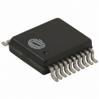
W682510RG Nuvoton Technology Corporation of America, W682510RG Datasheet - Page 9

W682510RG
Manufacturer Part Number
W682510RG
Description
IC VOICEBAND CODEC 5V 2CH 20SSOP
Manufacturer
Nuvoton Technology Corporation of America
Type
PCMr
Datasheet
1.W682510E.pdf
(35 pages)
Specifications of W682510RG
Data Interface
PCM Audio Interface
Resolution (bits)
8 b
Number Of Adcs / Dacs
2 / 2
Sigma Delta
No
Voltage - Supply, Analog
4.5 V ~ 5.5 V
Voltage - Supply, Digital
4.5 V ~ 5.5 V
Operating Temperature
-40°C ~ 85°C
Mounting Type
Surface Mount
Package / Case
20-SSOP
For Use With
W682510DK - KIT DEVELOPMENT FOR W682510
Lead Free Status / RoHS Status
Lead free / RoHS Compliant
Law format. The μ-Law or A-Law format is pin-selectable through the μ/A-Law pin. The compression
format can be selected according to Table 7.1.
The digital 8-bit μ-Law or A-Law samples are fed to the PCM interface for serial or parallel
transmission at the sample rate supplied by the external frame sync FST.
AI1 and AI2 are the transmit analog inputs for channels 1 and 2. AO1- and AO2- are the transmit level
feedback for channels 1 and 2. AI1 and AI2 are inverting inputs for the Op-Amps. AO1- and AO2- are
connected to the outputs of the Op-Amps and are used to set the level, as illustrated below. When AI1
and AI2 are not used, connect AI1 to AO1- and AI2 to AO2-. During power saving mode and power
down mode, the AO1- and AO2- outputs are tied weakly to V
impedance on the W682310 (See table on page 14).
The PCM signal output of channel 1 when the parallel mode is selected. The PCM output signal is
sent from PCMT1 in a sequential order, synchronizing with the rising edge of the BCLK signal. The
MSB may be output at the rising edge of the FST signal, based on the timing between BCLK and FST.
This output pin is in a high impedance state except during 8-bit PCM output. It is also in a high
impedance state during power-saving state or power-down. When serial operation is selected, this pin
is configured to be the output of the serial multiplexed two channel PCM signal. A pull-up resistor must
CH1 Analog Input
CH1 Analog Input
CH2 Analog Input
CH2 Analog Input
7.1.1. AI1, AI2, AO1-, AO2-
7.1.2. PCMT1
μ/A-Law Pin
V
V
DD
SSA
C1
C1
C1
C1
C2
C2
C2
C2
TABLE 7.1: PIN-SELECTABLE COMPRESSION FORMAT
(HIGH)
(LOW)
R1
R1
R1
R1
R3
R3
R3
R3
R2
R2
R2
R2
R4
R4
R4
R4
AO1-
AO1-
AO1-
AO1-
AI1
AI1
AI1
AI1
AO2-
AO2-
AO2-
AO2-
AI2
AI2
AI2
AI2
+
+
+
+
+
+
+
+
- 9 -
-
-
-
-
-
-
-
-
Format
μ-Law
A-Law
SSA
Publication Release Date: April 2005
W682510/W682310
on the W682510 or are high
Gain=R4/R3 ≤ 10
Gain=R4/R3 ≤ 10
R4 > 20 k Ohm
R4 > 20 k Ohm
Gain=R2/R1 ≤ 10
Gain=R2/R1 ≤ 10
R2 > 20 k Ohm
R2 > 20 k Ohm
Revision A10


