W682510RG Nuvoton Technology Corporation of America, W682510RG Datasheet - Page 7
W682510RG
Manufacturer Part Number
W682510RG
Description
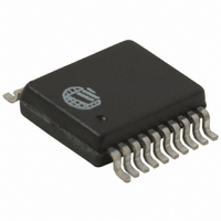
IC VOICEBAND CODEC 5V 2CH 20SSOP
Manufacturer
Nuvoton Technology Corporation of America
Type
PCMr
Datasheet
1.W682510E.pdf
(35 pages)
Specifications of W682510RG
Data Interface
PCM Audio Interface
Resolution (bits)
8 b
Number Of Adcs / Dacs
2 / 2
Sigma Delta
No
Voltage - Supply, Analog
4.5 V ~ 5.5 V
Voltage - Supply, Digital
4.5 V ~ 5.5 V
Operating Temperature
-40°C ~ 85°C
Mounting Type
Surface Mount
Package / Case
20-SSOP
For Use With
W682510DK - KIT DEVELOPMENT FOR W682510
Lead Free Status / RoHS Status
Lead free / RoHS Compliant


Pin
Name
V
RO2
RO1
PUI
PCMMS
V
V
FSR
PCMR2
PCMR1
PCMT1
PCMT2
FST
BCLK
V
μ/A-Law
AI1
AO1-
AO2-
AI2
REF
DD
SSD
SSA
6. PIN DESCRIPTION
1
2
3
4
5
6
7
8
9
10
11
12
13
14
15
16
17
18
19
20
SSOP
Pin #
PDIP
1
2
4
5
6
8
9
10
11
12
13
14
15
16
18
19
21
22
23
24
Pin #
SOP
Functionality
(CH1 = Channel 1, CH2 = Channel 2)
This pin is used to bypass the signal ground. It needs to be decoupled to V
through a 0.1 μF ceramic decoupling capacitor. No external loads should be
tied to this pin.
CH2 Non-Inverting output of the receive smoothing filter. This pin can typically
drive a 600 Ω load (W682510) or 1200 Ω load (W682310).
CH1 Non-Inverting output of the receive smoothing filter. This pin can typically
drive a 600 Ω load (W682510) or 1200 Ω load (W682310)..
Power up input signal. When this pin is HIGH (tied to V
up. When LOW (tied to V
PCM mode select input (serial or parallel data interface) HIGH = Parallel, LOW
= Serial
Power supply. This pin should be decoupled to V
capacitor.
This is the digital supply ground. This pin should be connected to 0V.
8 kHz Frame Sync input for the PCM receive section. It can also be connected
to the FST pin when transmit and receive are synchronous operations.
CH2 PCM input data receive pin. The data needs to be synchronous with the
FSR and BCLK pins.
CH1 PCM input data receive pin. The data needs to be synchronous with the
FSR and BCLK pins.
CH1 PCM output data transmit pin. The output data is synchronous with the
FST and BCLK pins.
CH2 PCM output data transmit pin. The output data is synchronous with the
FST and BCLK pins.
8 kHz transmit frame sync input. This pin synchronizes the transmit data bytes.
PCM transmit and receive bit clock input pin for CH1 and CH2 transmit.
This is the analog supply ground. This pin should be connected to 0V.
Compander mode select pin. μ-Law companding is selected when this pin is
LOW (tied to V
V
CH1 Non-Inverting input of the first gain stage in the transmit path.
CH1 Inverting analog output of the first gain stage in the transmit path.
CH2 Inverting analog output of the first gain stage in the transmit path
CH2 Non-Inverting input of the first gain stage in the transmit path.
DD
.)
SS
.) A-Law companding is selected when pin is HIGH (tied to
- 7 -
SS
) the part is powered down.
Publication Release Date: April 2005
W682510/W682310
SS
with a 0.1μF ceramic
DD
) the part is powered
Revision A10
SS
Related parts for W682510RG
Image
Part Number
Description
Manufacturer
Datasheet
Request
R

Part Number:
Description:
Manufacturer:
Nuvoton Technology Corporation of America
Datasheet:
Part Number:
Description:
Manufacturer:
Nuvoton Technology Corporation of America
Datasheet:
Part Number:
Description:
Manufacturer:
Nuvoton Technology Corporation of America
Datasheet:
Part Number:
Description:
Manufacturer:
Nuvoton Technology Corporation of America
Datasheet:
Part Number:
Description:
Manufacturer:
Nuvoton Technology Corporation of America
Datasheet:
Part Number:
Description:
Manufacturer:
Nuvoton Technology Corporation of America
Datasheet:
Part Number:
Description:
Manufacturer:
Nuvoton Technology Corporation of America
Datasheet: