W681360SG TR Nuvoton Technology Corporation of America, W681360SG TR Datasheet - Page 7
W681360SG TR
Manufacturer Part Number
W681360SG TR
Description
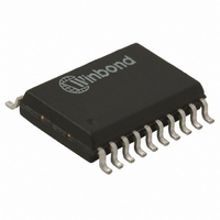
IC VOICEBAND CODEC 3V 1CH 20SOP
Manufacturer
Nuvoton Technology Corporation of America
Type
PCMr
Datasheet
1.W681360YG.pdf
(34 pages)
Specifications of W681360SG TR
Data Interface
PCM Audio Interface
Resolution (bits)
13 b
Number Of Adcs / Dacs
1 / 1
Sigma Delta
No
Voltage - Supply, Analog
2.7 V ~ 5.25 V
Voltage - Supply, Digital
2.7 V ~ 5.25 V
Operating Temperature
-40°C ~ 85°C
Mounting Type
Surface Mount
Package / Case
20-SOP
For Use With
W681360ES - KIT EVAL FOR W681360
Lead Free Status / RoHS Status
Lead free / RoHS Compliant
Other names
W681360SG T&R
W681360SG T&R
W681360SG T&R


Pin
Name
V
RO-
PAI
PAO-
PAO+
V
FSR
PCMR
BCLKR
PUI
MCLK
BCLKT
PCMT
FST
V
HB
AO
AI-
AI+
V
REF
DD
SS
AG
6. PIN DESCRIPTION
Pin No.
non-
QFN
1
2
3
4
5
6
7
8
9
10
11
12
13
14
15
16
17
18
19
20
QFN
30
1
2
3
5
6
7
8
9
12
13
16
17
19
20
22
23
24
26
29
Functionality
This pin is used to bypass the on–chip V
This pin should be bypassed to V
inductance traces. The V
V
Inverting output of the receive smoothing filter. This pin can typically drive a 2kΩ load to
0.886V
Inverting input to the power amplifier. The non-inverting input is tied internally to V
voltage.
Inverting power amplifier output. The PAO- and PAO+ can drive a 300Ω load differentially
to 1.772V
Non-inverting power amplifier output. The PAO- and PAO+ can drive a 300Ω load
differentially to 1.772V
Power supply. Should be decoupled to V
8kHz Frame Sync input for the PCM receive section. FSR can be asynchronous to FST in
either Long Frame Sync or Short Frame Sync mode.
PCM input data receive pin. The data needs to be synchronous with the FSR and BCLKR
pins.
PCM receive bit clock input pin. Can accept any bit clock frequency from 256 to 4800kHz.
When not clocked it can be used to select the 16 sign-bit extended synchronous mode
(BCLKR=0) or the receive gain adjust synchronous mode (BCLKR=1)
Power up input signal. When this pin is tied to V
V
System master clock input. Possible input frequencies are 256kHz, 512kHz, 1536kHz,
1544kHz, 2048kHz, 2560kHz, 4096kHz & 4800kHz. For performance reasons, it is
recommended that MCLK be synchronous and aligned to the FST signal. This is a
requirement in the case of 256 and 512kHz frequencies.
PCM transmit bit clock input pin. Can accept any bit clock frequency from 256 to
4800kHz.
PCM output data transmit pin. The output data is synchronous with the FST and BCLKT
pins.
8kHz transmit frame sync input. This pin synchronizes the transmit data bytes.
This is the supply ground. This pin should be connected to 0V.
High-pass Bypass. Determines if the transmit high-pass filter is used (HB=’0’) or
bypassed (HB=’1’). When the high pass is bypassed the frequency response extends to
DC.
Analog output of the first gain stage in the transmit path.
Inverting input of the first gain stage in the transmit path.
Non-inverting input of the first gain stage in the transmit path.
Mid-Supply analog ground pin, which supplies a V
analog signal processing. This pin should be decoupled to V
This pin becomes high impedance when the chip is powered down.
AG
SS
, the part is powered down.
pin. Nothing is to be connected to this pin except the bypass capacitor.
PEAK
PEAK
referenced to analog ground.
.
PEAK
REF
.
- 7 -
pin is only used for generating the reference voltage for the
SS
with a 0.1μF ceramic capacitor using short, low
DD
Publication Release Date: September 2005
SS
/2 voltage reference for the V
with a 0.1μF ceramic capacitor.
DD
, the part is powered up. When tied to
DD
/2 volt reference voltage for all-
SS
with a 0.01μF capacitor.
W681360
Revision A.2
AG
output pin.
AG
Related parts for W681360SG TR
Image
Part Number
Description
Manufacturer
Datasheet
Request
R

Part Number:
Description:
Manufacturer:
Nuvoton Technology Corporation of America
Datasheet:
Part Number:
Description:
Manufacturer:
Nuvoton Technology Corporation of America
Datasheet:
Part Number:
Description:
Manufacturer:
Nuvoton Technology Corporation of America
Datasheet:
Part Number:
Description:
Manufacturer:
Nuvoton Technology Corporation of America
Datasheet:
Part Number:
Description:
Manufacturer:
Nuvoton Technology Corporation of America
Datasheet:
Part Number:
Description:
Manufacturer:
Nuvoton Technology Corporation of America
Datasheet:
Part Number:
Description:
Manufacturer:
Nuvoton Technology Corporation of America
Datasheet: