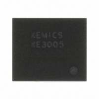
XE3005I064TRLF Semtech, XE3005I064TRLF Datasheet - Page 15

XE3005I064TRLF
Manufacturer Part Number
XE3005I064TRLF
Description
IC CODEC LOW PWR 16BIT 20-UCSP
Manufacturer
Semtech
Type
Audio Codecr
Datasheet
1.XE3005I064TRLF.pdf
(37 pages)
Specifications of XE3005I064TRLF
Data Interface
Serial
Resolution (bits)
16 b
Number Of Adcs / Dacs
1 / 1
Sigma Delta
Yes
S/n Ratio, Adcs / Dacs (db) Typ
78 / 78
Dynamic Range, Adcs / Dacs (db) Typ
78 / 78
Voltage - Supply, Analog
1.8 V ~ 3.6 V
Voltage - Supply, Digital
1.8 V ~ 3.6 V
Operating Temperature
-20°C ~ 70°C
Mounting Type
Surface Mount
Package / Case
20-UCSP®
Lead Free Status / RoHS Status
Lead free / RoHS Compliant
Other names
XE3005I064TR
Using the SPI pins at startup the user is able to configure the CODEC in the corresponding setups without
reprogramming through the SPI interface and protocol. In best case the SPI interface can then be completely omitted and
the 3 SPI pins can be fixed to ‘0’ or ‘1’.
Once the device has been powered up, the configuration registers can be modified at all times (also when the device is
active) through the SPI interface.
The following section describes the SPI protocol which is required to change the control registers from their default
values.
3.3
The serial peripheral interface (SPI) allows the device to communicate synchronously with other devices such as a
microprocessor or a DSP. The CODEC interface only implements a slave controller. This section describes the
communication from master (e.g. DSP) to slave (CODEC pin MOSI) and from slave (CODEC pin MISO) to a master (e.g.
DSP).
Four lines are used to transmit data between the slave and master:
-
-
-
-
3.3.1
During SPI communication, data is simultaneously transmitted and received.
The master puts data on the MOSI line on the falling edge of SCK; the slave reads the data on the rising edge of SCK.
The slave puts data on the MISO line on the falling edge of SCK; the master reads the data on the rising edge of SCK.
Transmission in either direction is by 2 bytes with MSB first.
The SS pin should be kept low during the whole transfer of data.
There are three timing constraints:
© Semtech 2005
2. Programming through SPI interface after power-up
MOSI (Master Out, Slave In) data from master to slave, synchronous with the SPI clock (SCK).
MISO (Master In, Slave Out) data from slave to master, synchronous with the SPI clock (SCK).
SCK (Serial Clock) synchronizes the data bits of MOSI and MISO.
SS (Slave Select) Slave devices are selected by activating SS.
SERIAL PERIPHERAL INTERFACE - SPI
-
Protocol
Recovery time (t
MOSI
MISO
SCK
SS
t
recovery
15
15
recovery
14
14
) between the falling edge of SS and the falling edge of SCK.
…
…
Figure 16: SPI signal timing
15
1/F
sck
XE3005/XE3006
…
…
1
1
t
disable
0
0
www.semtech.com


