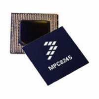
MPC8245LZU333D Freescale Semiconductor, MPC8245LZU333D Datasheet - Page 47

MPC8245LZU333D
Manufacturer Part Number
MPC8245LZU333D
Description
IC MPU 32BIT 333MHZ 352-TBGA
Manufacturer
Freescale Semiconductor
Series
PowerQUICC IIr
Specifications of MPC8245LZU333D
Processor Type
MPC82xx PowerQUICC II 32-bit
Speed
333MHz
Voltage
2V
Mounting Type
Surface Mount
Package / Case
352-TBGA
Core Size
32 Bit
Program Memory Size
32KB
Cpu Speed
333MHz
Embedded Interface Type
I2C
Digital Ic Case Style
TBGA
No. Of Pins
352
Supply Voltage Range
1.9V To 2.2V
Rohs Compliant
No
Family Name
MPC82XX
Device Core
PowerPC
Device Core Size
64b
Frequency (max)
333MHz
Instruction Set Architecture
RISC
Supply Voltage 1 (typ)
2/2.1/3.3V
Operating Supply Voltage (max)
2.2/3.465V
Operating Supply Voltage (min)
1.9/3.135V
Operating Temp Range
0C to 105C
Operating Temperature Classification
Commercial
Mounting
Surface Mount
Pin Count
352
Package Type
TBGA
Lead Free Status / RoHS Status
Contains lead / RoHS non-compliant
Features
-
Lead Free Status / Rohs Status
Not Compliant
Available stocks
Company
Part Number
Manufacturer
Quantity
Price
Company:
Part Number:
MPC8245LZU333D
Manufacturer:
FREE
Quantity:
12
Company:
Part Number:
MPC8245LZU333D
Manufacturer:
MOTOROLA
Quantity:
648
Company:
Part Number:
MPC8245LZU333D
Manufacturer:
Freescale Semiconductor
Quantity:
10 000
Part Number:
MPC8245LZU333D
Manufacturer:
MOTOROLA/摩托罗拉
Quantity:
20 000
System Design
SRESET, TRIG_IN, and TRIG_OUT. The default state (logic 1) of SDMA1 selects the MPC8240
backward-compatible mode functionality, while a logic 0 state on the SDMA1 signal selects extended
ROM functionality. In extended ROM mode, the TBEN, CHKSTOP_IN, SRESET, TRIG_IN, and
TRIG_OUT functionalities are not available.
The driver names and pin capability of the MPC8245 and the MPC8240 differ slightly. Refer to the drive
capability table (for the ODCR register at 0x73) in the MPC8240 Integrated Processor Hardware
Specifications and
Table
4.
The programmable PCI output valid and output hold feature controlled by bits in the power management
configuration register 2 (PMCR2) <0x72> differs slightly in the MPC8245. For the MPC8240, three bits,
PMCR2[6:4] = PCI_HOLD_DEL, are used to select 1 of 8 possible PCI output timing configurations.
PMCR2[6:5] are software-controllable but are initially set by the reset configuration state of the MCP and
CKE signals, respectively. Software can change PMCR2[4]. The default configuration for PMCR2[6:4] =
0b110 since the MCP and CKE signals have internal pull-up resistors, but this default configuration does
not select 33- or 66-MHz PCI operation output timing parameters for the MPC8240. Software makes this
selection. For the MPC8245, only two bits in the power management configuration register 2 (PMCR2),
PMCR2[5:4] = PCI_HOLD_DEL, control the variable PCI output timing. PMCR2[5:4] are software
controllable but are initially set by the inverted reset configuration state of the MCP and CKE signals,
respectively. The default configuration for PMCR2[5:4] = 0b00 since the MCP and CKE signals have
internal pull-up resistors and the values from these signals are inverted; this default configuration selects
66-MHz PCI operation output timing parameters. There are four programmable PCI output timing
configurations on the MPC8245. See
Table
11.
Voltage sequencing requirements for the MPC8245 are similar to those for the MPC8240, with two
exceptions in the MPC8245. In the MPC8245, the non-PCI input voltages (V
) must not be greater than
in
GV
or OV
by more than 0.6 V at all times, including during power-on reset (see Caution 5 in
DD
DD
Table
2). Second, LV
must not exceed OV
by more than 3.0 V at any time, including during
DD
DD
power-on reset (see Caution 10 in
Table
2); the allowable separation between LV
and OV
is 3.6 V
DD
DD
for the MPC8240.
There is no LAV
input voltage supply signal on the MPC8245 since the SDRAM clock delay-locked
DD
loop (DLL) has power supplied internally. Signal D17 should be treated as a NC for the MPC8245.
Application note AN2128 highlights the differences between the MPC8240 and the MPC8245.
7.7
JTAG Configuration Signals
Boundary scan testing is enabled through the JTAG interface signals. The TRST signal is optional in the
IEEE 1149.1 specification but is provided on all processors that implement the Power Architecture
technology. While the TAP controller can be forced to the reset state using only the TCK and TMS signals,
more reliable power-on reset performance can be obtained if the TRST signal is asserted during power-on
reset. Because the JTAG interface is also used for accessing the common on-chip processor (COP)
function, simply tying TRST to HRESET is not practical.
The COP function of these processors allows a remote computer system (typically, a PC with dedicated
hardware and debugging software) to access and control the internal operations of the processor. The COP
interface connects primarily through the JTAG, with additional status monitoring signals. The COP port
must independently assert HRESET or TRST to control the processor. If the target system has independent
MPC8245 Integrated Processor Hardware Specifications, Rev. 10
Freescale Semiconductor
47


