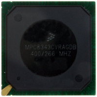
MPC8343CVRAGDB Freescale Semiconductor, MPC8343CVRAGDB Datasheet - Page 77

MPC8343CVRAGDB
Manufacturer Part Number
MPC8343CVRAGDB
Description
IC MPU PWRQUICC II 620-PBGA
Manufacturer
Freescale Semiconductor
Datasheet
1.MPC8343VRAGDB.pdf
(79 pages)
Specifications of MPC8343CVRAGDB
Processor Type
MPC83xx PowerQUICC II Pro 32-Bit
Speed
400MHz
Voltage
1.2V
Mounting Type
Surface Mount
Package / Case
620-PBGA
For Use With
CWH-PPC-8343N-VX - KIT EVAL SYSTEM QUICCSTART 8248CWH-PPC-8343N-VE - EVALUATION SYSTEM QUICC MPC8343E
Lead Free Status / RoHS Status
Lead free / RoHS Compliant
Features
-
Available stocks
Company
Part Number
Manufacturer
Quantity
Price
Company:
Part Number:
MPC8343CVRAGDB
Manufacturer:
Freescale Semiconductor
Quantity:
10 000
23 Document Revision History
Table 64
Freescale Semiconductor
Number
Rev.
10
9
8
7
6
5
4
provides a revision history of this document.
MPC8343EA PowerQUICC II Pro Integrated Host Processor Hardware Specifications, Rev. 10
11/2010
05/2010
12/2006
5/2009
2/2009
4/2007
3/2007
Date
Table 19, “DDR and DDR2 SDRAM Output AC Timing Specifications,” modified T
from 900 ps to 775 ps.
• In
• In
• In
• Added
• In
• In
• In
• Added footnote 6 to
• In
• In
• Added footnote 10 to
• In
• In
• In
• In
• In
• In
• Deleted Section 21.8, “JTAG Configuration Signals,” and Figure 43, “JTAG Interface Connection.”
• Page 1, updated first paragraph to reflect PowerQUICC II Pro information.
• In Table 18, “DDR and DDR2 SDRAM Input AC Timing Specifications,” added note 2 to t
• In Figure 38, “JTAG Interface Connection,” updated with new figure.
• In Figure 38, “JTAG Interface Connection,” updated with new figure.
• In Section 23, “Ordering Information,” replaced first paragraph and added a note.
• In Section 23.1, “Part Numbers Fully Addressed by this Document,” replaced first paragraph.
and PBGA from 95.5 Sn/0.5 Cu/4 Ag to 96.5 Sn/3.5 Ag.
and DDR2.
in DLL bypass mode). Similarly, made the same correction to
for output signals.
resistor. For proper functionality of the device, this pin must be pulled up or actively driven high
during a hard reset. No external pull-down resistors are allowed to be attached to this net.”
independent filter circuits,” and “the five AVDD pins” to provide four independent filter circuits,” and
“the four AVDD pins.”
is limited to 400 with a platform frequency of 266.”
added USB to the seventh row.
paragraph, added a new paragraph.
and deleted original note 3; renumbered the remaining notes.
Section 18.1, “Package Parameters for the MPC8343EA
Table
Table
Table
Table
Section 21.7, “Pull-Up Resistor
Table 25
Table
Section 9.2, “USB AC Electrical
Table
Section 21.1, “System
Section 21.2, “PLL Power Supply
Table
Section 21.7, “Pull-Up Resistor
Table
62, footnote 1, changed 667(TBGA) to 533(TBGA). footnote 4, added data rate for DDR1
35, corrected t
62, updated note 1 to say the following: “For temperature range = C, processor frequency
51, added overbar to LCS[4] and LCS[5] signals. In
53, added two columns for the DDR1 and DDR2 memory bus frequency.
51, updated note 11 to say the following: “SEC1_TXD[3] is required an external pull-up
3,
Table 64. Document Revision History
“Output Drive Capability,”
through
8, “EC_GTX_CLK125 AC Timing Specifications.”
Table
Table
Table
LBKHOV
Clocking,” removed “(AVDD1)” and “(AVDD2”) from bulleted list.
26, changed V
7.
51.
parameter to t
Requirements, updated the list of open drain type pins.
Requirements,“ deleted last two paragraphs and after first
Substantive Change(s)
Specifications,” clarified that AC table is for ULPI only.
Filtering,” in the second paragraph, changed “provide five
changed the values in the Output Impedance column and
IL
(min) to V
LBKLOV
(output data is driven on falling edge of clock
IH
(max) to (20%–80%).
PBGA, changed solder ball for TBGA
Table 51
Figure
17,
added note for pin LGPL4.
Document Revision History
Figure
ddkhds
19, and
for 333 MHz
Figure 20
CISKEW
77


