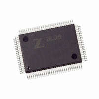
Z8018233FSC Zilog, Z8018233FSC Datasheet - Page 77

Z8018233FSC
Manufacturer Part Number
Z8018233FSC
Description
IC 33MHZ STATIC MIMIC 100-QFP
Manufacturer
Zilog
Datasheet
1.Z8018233FSG.pdf
(109 pages)
Specifications of Z8018233FSC
Processor Type
Z180
Features
Smart Peripheral Controller
Speed
33MHz
Voltage
5V
Mounting Type
Surface Mount
Package / Case
100-QFP
Processor Series
Z8018xx
Core
Z80
Data Bus Width
8 bit
Program Memory Type
ROMLess
Interface Type
UART
Maximum Clock Frequency
33 MHz
Number Of Programmable I/os
24
Number Of Timers
2
Operating Supply Voltage
4.5 V to 5.5 V
Maximum Operating Temperature
+ 70 C
Mounting Style
SMD/SMT
Minimum Operating Temperature
0 C
Lead Free Status / RoHS Status
Contains lead / RoHS non-compliant
Available stocks
Company
Part Number
Manufacturer
Quantity
Price
Company:
Part Number:
Z8018233FSC
Manufacturer:
ZILOG
Quantity:
591
The data direction register determines which are inputs
and outputs in the PC Data Register. When a bit is set to 1
the corresponding bit in the PC Data Register is an input.
If the bit is 0, then the corresponding bit is an output.
16550 MIMIC INTERFACE DMA
DS971820600
The 16550 MIMIC is also able to do direct DMA with the
PC/XT/AT. DMA is enabled by setting bits 3, 4 and 5 of the
Master Control Register. DMA is accomplished by using
the two DMA pins and the Transmitter Holding and Receive
Data Registers.
If bit 5 is 1, the /HTxRDY pin is equal to the complement of
the Transmit Holding Register Empty bit. If bit 5 is 1 and bit
3 is 0 the external /DREQ1 pin of the Z180 MPU is disabled
and the internal /DREQ1 is equal to the complement of the
Transmit Holding Register Empty Shadow bit. If bit 5 is 1
and bit 3 is 1 the external /DREQ0 pin of the Z180 MPU is
Zilog
D7
X
D6 D5 D4 D3 D2 D1
X
(Z180 MPU Read/Write, Address xxDEH)
X
Figure 88. PC, Port C, Data Register
X
X
X
X
D0
X
PC Data Register
/INT2, /INT1 Read Ext Data
Write b7=1 Clears /INT2 Edge
Write b6=1 Clears /INT1 Edge
PS009801-0301
P R E L I M I N A R Y
When the Z180 MPU writes to the PC Data Register, the
data is stored in the internal buffer. The values of Port C
data register are undefined after reset. Any bits that are
output are then sent on to the output buffers.
When the Z180 MPU reads the PC Data Register, the data
on the external pins is returned.
Bits 6 and 7 serve the special function of reading the value
of the external /INT2 and /INT1 lines. When operating
either /INT2 or /INT1 in edge detection mode, the edge
detect latch is reset by writing a 1 to bit 6 or 7 respectively.
Writing a 0 has no effect. These latches should be reset
at the end of an /INT1 or /INT2 interrupt service routine
when using edge-triggered interrupt modes.
disabled and the internal /DREQ0 is equal to the
complement of the Transmit Holding Register Empty
Shadow bit.
If bit 4 is 1, then the /HRxRDY pin is equal to the complement
of the Data Ready bit. If bit 4 is 1 and bit 3 is 0 the external
/DREQ0 pin of the Z180 MPU is disabled and the internal
/DREQ0 is equal to the complement of the Data Ready
Shadow bit. If bit 4 is 1 and bit 3 is 1 the external /DREQ1
pin of the Z180 MPU is disabled and the internal /DREQ1
is equal to the complement or the Data Ready Shadow bit.
Z
ILOG
I
NTELLIGENT
Z80182/Z8L182
P
ERIPHERAL
3-77


