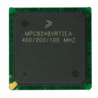
MPC8248VRTIEA Freescale Semiconductor, MPC8248VRTIEA Datasheet - Page 18

MPC8248VRTIEA
Manufacturer Part Number
MPC8248VRTIEA
Description
IC MPU POWERQUICC II 516-PBGA
Manufacturer
Freescale Semiconductor
Datasheet
1.MPC8248VRMIBA.pdf
(60 pages)
Specifications of MPC8248VRTIEA
Processor Type
MPC82xx PowerQUICC II 32-bit
Speed
400MHz
Voltage
1.5V
Mounting Type
Surface Mount
Package / Case
516-PBGA
Family Name
MPC82XX
Device Core
PowerQUICC II
Device Core Size
32b
Frequency (max)
400MHz
Instruction Set Architecture
RISC
Supply Voltage 1 (typ)
1.5V
Operating Supply Voltage (max)
1.575V
Operating Supply Voltage (min)
1.425V
Operating Temp Range
0C to 105C
Operating Temperature Classification
Commercial
Mounting
Surface Mount
Pin Count
516
Package Type
TEPBGA
For Use With
CWH-PPC-8248N-VE - KIT EVAL SYSTEM QUICCSTART 8248
Lead Free Status / RoHS Status
Lead free / RoHS Compliant
Features
-
Lead Free Status / Rohs Status
Compliant
Available stocks
Company
Part Number
Manufacturer
Quantity
Price
Company:
Part Number:
MPC8248VRTIEA
Manufacturer:
Freescale Semiconductor
Quantity:
10 000
Part Number:
MPC8248VRTIEA
Manufacturer:
FREESCALE
Quantity:
20 000
AC Electrical Characteristics
Figure 4
Figure 5
18
FCC output signals
FCC output signals
Note: When GFMR[TCI] = 0
Note: When GFMR[TCI] = 1
FCC input signals
shows the FCC external clock.
shows the SCC/SMC/SPI/I
SCC/SMC/SPI/I2C output signals
SCC/SMC/SPI/I2C input signals
Serial ClKin
(See note)
(See note)
MPC8272 PowerQUICC II™ Family Hardware Specifications, Rev. 2
Note: There are four possible timing conditions for SPI:
Note: There are two possible timing conditions for SCC/SMC/I
1. Input sampled on the rising edge and output driven on the rising edge.
2. Input sampled on the rising edge and output driven on the falling edge.
3. Input sampled on the falling edge and output driven on the falling edge (shown).
4. Input sampled on the falling edge and output driven on the rising edge.
1. Input sampled on the falling edge and output driven on the falling edge (shown).
2. Input sampled on the falling edge and output driven on the rising edge.
Figure 5. SCC/SMC/SPI/I
Serial CLKin
sp16b
Figure 4. FCC External Clock Diagram
2
C external clock.
sp18b
2
sp36b/sp37b
C External Clock Diagram
sp17b
sp38b/sp39b
sp19b
2
C:
sp36b/sp37b
new CLKin
Freescale Semiconductor


