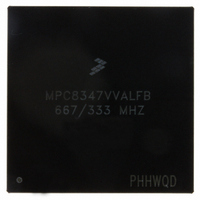
MPC8347VVALFB Freescale Semiconductor, MPC8347VVALFB Datasheet - Page 52

MPC8347VVALFB
Manufacturer Part Number
MPC8347VVALFB
Description
IC MPU POWERQUICC II 672-TBGA
Manufacturer
Freescale Semiconductor
Series
PowerQUICC II PROr
Specifications of MPC8347VVALFB
Processor Type
MPC83xx PowerQUICC II Pro 32-Bit
Speed
667MHz
Voltage
1.3V
Mounting Type
Surface Mount
Package / Case
672-TBGA
Processor Series
MPC8xxx
Core
e300
Data Bus Width
32 bit
Development Tools By Supplier
MPC8349E-MITXE
Maximum Clock Frequency
667 MHz
Maximum Operating Temperature
+ 105 C
Mounting Style
SMD/SMT
I/o Voltage
1.8 V, 2.5 V, 3.3 V
Minimum Operating Temperature
0 C
Family Name
MPC83xx
Device Core
PowerQUICC II Pro
Device Core Size
32b
Frequency (max)
667MHz
Instruction Set Architecture
RISC
Supply Voltage 1 (typ)
1.3V
Operating Supply Voltage (max)
1.36V
Operating Supply Voltage (min)
1.24V
Operating Temp Range
0C to 105C
Operating Temperature Classification
Commercial
Mounting
Surface Mount
Pin Count
672
Package Type
TBGA
Core Size
32 Bit
Program Memory Size
64KB
Cpu Speed
667MHz
Embedded Interface Type
I2C, SPI, USB, UART
Digital Ic Case Style
TBGA
No. Of Pins
672
Rohs Compliant
Yes
Lead Free Status / RoHS Status
Lead free / RoHS Compliant
Features
-
Lead Free Status / Rohs Status
Lead free / RoHS Compliant
Available stocks
Company
Part Number
Manufacturer
Quantity
Price
Company:
Part Number:
MPC8347VVALFB
Manufacturer:
VIOCR
Quantity:
114
Company:
Part Number:
MPC8347VVALFB
Manufacturer:
Freescale Semiconductor
Quantity:
10 000
Part Number:
MPC8347VVALFB
Manufacturer:
FREESCALE
Quantity:
20 000
SPI
17.2
Table 54
Figure 36
52
Input current
Output high voltage
Output low voltage
Output low voltage
SPI outputs valid—Master mode (internal clock) delay
SPI outputs hold—Master mode (internal clock) delay
SPI outputs valid—Slave mode (external clock) delay
SPI outputs hold—Slave mode (external clock) delay
SPI inputs—Master mode (internal clock input setup time
SPI inputs—Master mode (internal clock input hold time
SPI inputs—Slave mode (external clock) input setup time
SPI inputs—Slave mode (external clock) input hold time
Notes:
1. Output specifications are measured from the 50 percent level of the rising edge of CLKIN to the 50 percent level of the signal.
2. The symbols for timing specifications follow the pattern of t
Timings are measured at the pin.
and t
(NI) for the time SPICLK clock reference (K) goes to the high state (H) until outputs (O) are invalid (X).
(first two letters of functional block)(reference)(state)(signal)(state)
provides the SPI input and output AC timing specifications.
SPI AC Timing Specifications
provides the AC test load for the SPI.
MPC8347EA PowerQUICC II Pro Integrated Host Processor Hardware Specifications, Rev. 11
Parameter
Output
Parameter
Table 53. SPI DC Electrical Characteristics (continued)
Table 54. SPI AC Timing Specifications
Figure 36. SPI AC Test Load
Z
Symbol
0
V
V
V
= 50 Ω
I
IN
OH
OL
OL
for outputs. For example, t
(first two letters of functional block)(signal)(state)(reference)(state)
I
OH
I
I
OL
OL
Condition
= –8.0 mA
= 8.0 mA
= 3.2 mA
—
Symbol
t
t
t
t
t
t
NEKHOV
NEKHOX
t
t
NIKHOV
NIKHOX
NEIVKH
NEIXKH
R
NIIVKH
NIIXKH
L
= 50 Ω
2
1
NIKHOX
Min
2.4
—
—
—
OV
Min
0.5
—
—
2
4
0
4
2
DD
symbolizes the internal timing
/2
Freescale Semiconductor
Max
0.5
0.4
±5
Max
—
—
—
—
—
—
—
6
8
for inputs
Unit
Unit
μA
ns
ns
ns
ns
ns
ns
ns
ns
V
V
V


