MPC8347VVALFB Freescale Semiconductor, MPC8347VVALFB Datasheet - Page 14
MPC8347VVALFB
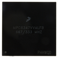
Manufacturer Part Number
MPC8347VVALFB
Description
IC MPU POWERQUICC II 672-TBGA
Manufacturer
Freescale Semiconductor
Series
PowerQUICC II PROr
Specifications of MPC8347VVALFB
Processor Type
MPC83xx PowerQUICC II Pro 32-Bit
Speed
667MHz
Voltage
1.3V
Mounting Type
Surface Mount
Package / Case
672-TBGA
Processor Series
MPC8xxx
Core
e300
Data Bus Width
32 bit
Development Tools By Supplier
MPC8349E-MITXE
Maximum Clock Frequency
667 MHz
Maximum Operating Temperature
+ 105 C
Mounting Style
SMD/SMT
I/o Voltage
1.8 V, 2.5 V, 3.3 V
Minimum Operating Temperature
0 C
Family Name
MPC83xx
Device Core
PowerQUICC II Pro
Device Core Size
32b
Frequency (max)
667MHz
Instruction Set Architecture
RISC
Supply Voltage 1 (typ)
1.3V
Operating Supply Voltage (max)
1.36V
Operating Supply Voltage (min)
1.24V
Operating Temp Range
0C to 105C
Operating Temperature Classification
Commercial
Mounting
Surface Mount
Pin Count
672
Package Type
TBGA
Core Size
32 Bit
Program Memory Size
64KB
Cpu Speed
667MHz
Embedded Interface Type
I2C, SPI, USB, UART
Digital Ic Case Style
TBGA
No. Of Pins
672
Rohs Compliant
Yes
Lead Free Status / RoHS Status
Lead free / RoHS Compliant
Features
-
Lead Free Status / Rohs Status
Lead free / RoHS Compliant
Available stocks
Company
Part Number
Manufacturer
Quantity
Price
Company:

Part Number:
MPC8347VVALFB
Manufacturer:
VIOCR
Quantity:
114
Company:
Part Number:
MPC8347VVALFB
Manufacturer:
Freescale Semiconductor
Quantity:
10 000
Part Number:
MPC8347VVALFB
Manufacturer:
FREESCALE
Quantity:
20 000


RESET Initialization
5.2
Table 10
14
Required assertion time of HRESET or SRESET (input) to activate reset flow
Required assertion time of PORESET with stable clock applied to CLKIN when the
MPC8347EA is in PCI host mode
Required assertion time of PORESET with stable clock applied to PCI_SYNC_IN
when the MPC8347EA is in PCI agent mode
HRESET/SRESET assertion (output)
HRESET negation to SRESET negation (output)
Input setup time for POR configuration signals (CFG_RESET_SOURCE[0:2] and
CFG_CLKIN_DIV) with respect to negation of PORESET when the MPC8347EA is
in PCI host mode
Input setup time for POR configuration signals (CFG_RESET_SOURCE[0:2] and
CFG_CLKIN_DIV) with respect to negation of PORESET when the MPC8347EA is
in PCI agent mode
Input hold time for POR configuration signals with respect to negation of HRESET
Time for the MPC8347EA to turn off POR configuration signals with respect to the
assertion of HRESET
Time for the MPC8347EA to turn on POR configuration signals with respect to the
negation of HRESET
Notes:
1. t
2. t
3. POR configuration signals consist of CFG_RESET_SOURCE[0:2] and CFG_CLKIN_DIV.
Output low voltage
Notes:
1. This table applies for pins PORESET, HRESET, SRESET, and QUIESCE.
2. HRESET and SRESET are open drain pins, thus V
to the CLKIN input, and PCI_SYNC_IN period depends on the value of CFG_CLKIN_DIV. See the MPC8349EA
PowerQUICC II Pro Integrated Host Processor Family Reference Manual.
PowerQUICC II Pro Integrated Host Processor Family Reference Manual.
PCI_SYNC_IN
CLKIN
is the clock period of the input clock applied to CLKIN. It is valid only in PCI host mode. See the MPC8349EA
provides the reset initialization AC timing specifications of the MPC8347EA.
RESET AC Electrical Characteristics
MPC8347EA PowerQUICC II Pro Integrated Host Processor Hardware Specifications, Rev. 11
is the clock period of the input clock applied to PCI_SYNC_IN. In PCI host mode, the primary clock is applied
Parameter
Table 9. RESET Pins DC Electrical Characteristics
Table 10. RESET Initialization Timing Specifications
Parameter
OH
Symbol
is not relevant for those pins.
V
OL
I
OL
Condition
= 3.2 mA
1
(continued)
Min
512
32
32
32
16
—
4
4
0
1
Min
—
Max
—
—
—
—
—
—
—
—
—
4
Freescale Semiconductor
Max
t
t
t
t
t
t
0.4
PCI_SYNC_IN
PCI_SYNC_IN
PCI_SYNC_IN
PCI_SYNC_IN
PCI_SYNC_IN
PCI_SYNC_IN
t
t
CLKIN
CLKIN
Unit
ns
ns
Unit
Notes
V
1, 3
—
1
2
1
1
1
2
1
3
Related parts for MPC8347VVALFB
Image
Part Number
Description
Manufacturer
Datasheet
Request
R

Part Number:
Description:
Integrated Host Processor Hardware Specifications
Manufacturer:
FREESCALE [Freescale Semiconductor, Inc]
Datasheet:

Part Number:
Description:
Manufacturer:
Freescale Semiconductor, Inc
Datasheet:
Part Number:
Description:
Manufacturer:
Freescale Semiconductor, Inc
Datasheet:
Part Number:
Description:
Manufacturer:
Freescale Semiconductor, Inc
Datasheet:
Part Number:
Description:
Manufacturer:
Freescale Semiconductor, Inc
Datasheet:
Part Number:
Description:
Manufacturer:
Freescale Semiconductor, Inc
Datasheet:
Part Number:
Description:
Manufacturer:
Freescale Semiconductor, Inc
Datasheet:
Part Number:
Description:
Manufacturer:
Freescale Semiconductor, Inc
Datasheet:
Part Number:
Description:
Manufacturer:
Freescale Semiconductor, Inc
Datasheet:
Part Number:
Description:
Manufacturer:
Freescale Semiconductor, Inc
Datasheet:
Part Number:
Description:
Manufacturer:
Freescale Semiconductor, Inc
Datasheet:
Part Number:
Description:
Manufacturer:
Freescale Semiconductor, Inc
Datasheet:
Part Number:
Description:
Manufacturer:
Freescale Semiconductor, Inc
Datasheet:
Part Number:
Description:
Manufacturer:
Freescale Semiconductor, Inc
Datasheet:
Part Number:
Description:
Manufacturer:
Freescale Semiconductor, Inc
Datasheet: