MPC8248VRPIEA Freescale Semiconductor, MPC8248VRPIEA Datasheet - Page 4
MPC8248VRPIEA
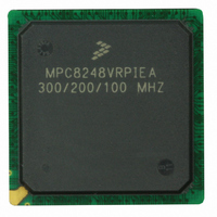
Manufacturer Part Number
MPC8248VRPIEA
Description
IC MPU POWERQUICC II 516-PBGA
Manufacturer
Freescale Semiconductor
Series
PowerQUICC IIr
Datasheet
1.MPC8248VRMIBA.pdf
(60 pages)
Specifications of MPC8248VRPIEA
Processor Type
MPC82xx PowerQUICC II 32-bit
Speed
300MHz
Voltage
1.5V
Mounting Type
Surface Mount
Package / Case
516-PBGA
Processor Series
MPC8xxx
Core
603e
Data Bus Width
32 bit
Maximum Clock Frequency
300 MHz
Operating Supply Voltage
1.4 V to 1.6 V
Maximum Operating Temperature
+ 105 C
Mounting Style
SMD/SMT
Data Ram Size
4 KB
Minimum Operating Temperature
0 C
Number Of Programmable I/os
14
Program Memory Size
16 KB
Program Memory Type
EEPROM
Core Size
32 Bit
Cpu Speed
300MHz
Embedded Interface Type
I2C, JTAG, SPI, UART
Digital Ic Case Style
BGA
No. Of Pins
516
Rohs Compliant
Yes
For Use With
CWH-PPC-8248N-VE - KIT EVAL SYSTEM QUICCSTART 8248
Lead Free Status / RoHS Status
Lead free / RoHS Compliant
Features
-
Lead Free Status / Rohs Status
Lead free / RoHS Compliant
Available stocks
Company
Part Number
Manufacturer
Quantity
Price
Company:

Part Number:
MPC8248VRPIEA
Manufacturer:
Freescale Semiconductor
Quantity:
135
Company:
Part Number:
MPC8248VRPIEA
Manufacturer:
Freescale Semiconductor
Quantity:
10 000


Overview
4
•
•
•
•
•
•
•
•
— Floating-point unit (FPU) supports floating-point arithmetic
— Support for cache locking
Low-power consumption
Separate power supply for internal logic (1.5 V) and for I/O (3.3 V)
Separate PLLs for G2_LE core and for the communications processor module (CPM)
— G2_LE core and CPM can run at different frequencies for power/performance optimization
— Internal core/bus clock multiplier that provides 2:1, 2.5:1, 3:1, 3.5:1, 4:1, 4.5:1, 5:1, 5.5:1, 6:1,
— Internal CPM/bus clock multiplier that provides 2:1, 2.5:1, 3:1, 3.5:1, 4:1, 5:1, 6:1 ,and 8:1
64-bit data and 32-bit address 60x bus
— Bus supports multiple master designs—up to two external masters
— Supports single transfers and burst transfers
— 64-, 32-, 16-, and 8-bit port sizes controlled by on-chip memory controller
60x-to-PCI bridge
— Programmable host bridge and agent
— 32-bit data bus, 66 MHz, 3.3 V
— Synchronous and asynchronous 60x and PCI clock modes
— All internal address space available to external PCI host
— DMA for memory block transfers
— PCI-to-60x address remapping
System interface unit (SIU)
— Clock synthesizer
— Reset controller
— Real-time clock (RTC) register
— Periodic interrupt timer
— Hardware bus monitor and software watchdog timer
— IEEE 1149.1 JTAG test access port
Eight bank memory controller
— Glueless interface to SRAM, page mode SDRAM, DRAM, EPROM, Flash, and other
— Byte write enables
— 32-bit address decodes with programmable bank size
— Three user programmable machines, general-purpose chip-select machine, and page mode
— Byte selects for 64-bit bus width (60x)
— Dedicated interface logic for SDRAM
Disable CPU mode
7:1, and 8:1 ratios
ratios
user-definable peripherals
pipeline SDRAM machine
MPC8272 PowerQUICC II™ Family Hardware Specifications, Rev. 2
Freescale Semiconductor
Related parts for MPC8248VRPIEA
Image
Part Number
Description
Manufacturer
Datasheet
Request
R

Part Number:
Description:
Mpc8248 Powerquicc Ii Integrated Communications Processor
Manufacturer:
Freescale Semiconductor, Inc
Datasheet:
Part Number:
Description:
Manufacturer:
Freescale Semiconductor, Inc
Datasheet:
Part Number:
Description:
Manufacturer:
Freescale Semiconductor, Inc
Datasheet:
Part Number:
Description:
Manufacturer:
Freescale Semiconductor, Inc
Datasheet:
Part Number:
Description:
Manufacturer:
Freescale Semiconductor, Inc
Datasheet:
Part Number:
Description:
Manufacturer:
Freescale Semiconductor, Inc
Datasheet:
Part Number:
Description:
Manufacturer:
Freescale Semiconductor, Inc
Datasheet:
Part Number:
Description:
Manufacturer:
Freescale Semiconductor, Inc
Datasheet:
Part Number:
Description:
Manufacturer:
Freescale Semiconductor, Inc
Datasheet:
Part Number:
Description:
Manufacturer:
Freescale Semiconductor, Inc
Datasheet:
Part Number:
Description:
Manufacturer:
Freescale Semiconductor, Inc
Datasheet:
Part Number:
Description:
Manufacturer:
Freescale Semiconductor, Inc
Datasheet:
Part Number:
Description:
Manufacturer:
Freescale Semiconductor, Inc
Datasheet:
Part Number:
Description:
Manufacturer:
Freescale Semiconductor, Inc
Datasheet:
Part Number:
Description:
Manufacturer:
Freescale Semiconductor, Inc
Datasheet: