MPC8248VRPIEA Freescale Semiconductor, MPC8248VRPIEA Datasheet - Page 20
MPC8248VRPIEA
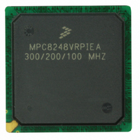
Manufacturer Part Number
MPC8248VRPIEA
Description
IC MPU POWERQUICC II 516-PBGA
Manufacturer
Freescale Semiconductor
Series
PowerQUICC IIr
Datasheet
1.MPC8248VRMIBA.pdf
(60 pages)
Specifications of MPC8248VRPIEA
Processor Type
MPC82xx PowerQUICC II 32-bit
Speed
300MHz
Voltage
1.5V
Mounting Type
Surface Mount
Package / Case
516-PBGA
Processor Series
MPC8xxx
Core
603e
Data Bus Width
32 bit
Maximum Clock Frequency
300 MHz
Operating Supply Voltage
1.4 V to 1.6 V
Maximum Operating Temperature
+ 105 C
Mounting Style
SMD/SMT
Data Ram Size
4 KB
Minimum Operating Temperature
0 C
Number Of Programmable I/os
14
Program Memory Size
16 KB
Program Memory Type
EEPROM
Core Size
32 Bit
Cpu Speed
300MHz
Embedded Interface Type
I2C, JTAG, SPI, UART
Digital Ic Case Style
BGA
No. Of Pins
516
Rohs Compliant
Yes
For Use With
CWH-PPC-8248N-VE - KIT EVAL SYSTEM QUICCSTART 8248
Lead Free Status / RoHS Status
Lead free / RoHS Compliant
Features
-
Lead Free Status / Rohs Status
Lead free / RoHS Compliant
Available stocks
Company
Part Number
Manufacturer
Quantity
Price
Company:

Part Number:
MPC8248VRPIEA
Manufacturer:
Freescale Semiconductor
Quantity:
135
Company:
Part Number:
MPC8248VRPIEA
Manufacturer:
Freescale Semiconductor
Quantity:
10 000


AC Electrical Characteristics
Figure 8
6.2
Table 11
20
PIO/IDMA/TIMER[TGATE assertion] input signals
shows PIO and timer signals.
lists SIU input characteristics.
SIU AC Characteristics
TIMER input signal [TGATE deassertion]
TIMER(sp42/43)/ PIO(sp42a/sp43a)
The CLKIN input to the MPC8272 should not exceed +/– 150 psec. This
represents total input jitter—the combination of short term (peak-to-peak)
and long term (cumulative). The duty cycle of CLKIN should not exceed the
ratio of 40:60.
Spread spectrum clocking is allowed with 1% input frequency down-spread
at maximum 60 KHz modulation rate regardless of input frequency.
The MPC8272 meets the timing requirements of PCI Specification Revision
2.2. Refer to
(Output Hold)” to determine if a specific clock configuration is compliant.
Note: TGATE is asserted on the rising edge of the clock; it is deasserted on the falling edge.
MPC8272 PowerQUICC II™ Family Hardware Specifications, Rev. 2
IDMA output signals
Section 7, “Clock Configuration
NOTE: CLKIN Jitter and Duty Cycle
NOTE: Spread Spectrum Clocking
output signals
Figure 8. PIO and Timer Signal Diagram
(See note)
(See note)
Sys clk
NOTE: PCI AC Timing
sp22
Modes,” and “Note: Tval
sp22
sp42/sp43
sp23
Freescale Semiconductor
sp42a/sp43a
sp42/sp43
sp23
Related parts for MPC8248VRPIEA
Image
Part Number
Description
Manufacturer
Datasheet
Request
R

Part Number:
Description:
Mpc8248 Powerquicc Ii Integrated Communications Processor
Manufacturer:
Freescale Semiconductor, Inc
Datasheet:
Part Number:
Description:
Manufacturer:
Freescale Semiconductor, Inc
Datasheet:
Part Number:
Description:
Manufacturer:
Freescale Semiconductor, Inc
Datasheet:
Part Number:
Description:
Manufacturer:
Freescale Semiconductor, Inc
Datasheet:
Part Number:
Description:
Manufacturer:
Freescale Semiconductor, Inc
Datasheet:
Part Number:
Description:
Manufacturer:
Freescale Semiconductor, Inc
Datasheet:
Part Number:
Description:
Manufacturer:
Freescale Semiconductor, Inc
Datasheet:
Part Number:
Description:
Manufacturer:
Freescale Semiconductor, Inc
Datasheet:
Part Number:
Description:
Manufacturer:
Freescale Semiconductor, Inc
Datasheet:
Part Number:
Description:
Manufacturer:
Freescale Semiconductor, Inc
Datasheet:
Part Number:
Description:
Manufacturer:
Freescale Semiconductor, Inc
Datasheet:
Part Number:
Description:
Manufacturer:
Freescale Semiconductor, Inc
Datasheet:
Part Number:
Description:
Manufacturer:
Freescale Semiconductor, Inc
Datasheet:
Part Number:
Description:
Manufacturer:
Freescale Semiconductor, Inc
Datasheet:
Part Number:
Description:
Manufacturer:
Freescale Semiconductor, Inc
Datasheet: