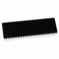
Z8018010PSG Zilog, Z8018010PSG Datasheet - Page 76

Z8018010PSG
Manufacturer Part Number
Z8018010PSG
Description
IC 10MHZ Z180 CMOS ENH MPU 64DIP
Manufacturer
Zilog
Specifications of Z8018010PSG
Processor Type
Z180
Features
8-Bit, Enhanced Z80 Megacell
Speed
10MHz
Voltage
5V
Mounting Type
Through Hole
Package / Case
64-DIP (0.750", 19.05mm)
Processor Series
Z8018xx
Core
Z80
Data Bus Width
8 bit
Maximum Clock Frequency
10 MHz
Number Of Timers
2
Operating Supply Voltage
0 V to 5 V
Maximum Operating Temperature
+ 70 C
Mounting Style
Through Hole
Minimum Operating Temperature
0 C
Core Size
8bit
Cpu Speed
10MHz
Digital Ic Case Style
DIP
No. Of Pins
64
Supply Voltage Range
4.5V To 5.5V
Operating Temperature Range
0°C To +70°C
Svhc
No SVHC (18-Jun-2010)
Base Number
8018010
Rohs Compliant
Yes
Clock Frequency
10MHz
Lead Free Status / RoHS Status
Lead free / RoHS Compliant
Other names
269-3889
Z8018010PSG
Z8018010PSG
Available stocks
Company
Part Number
Manufacturer
Quantity
Price
Company:
Part Number:
Z8018010PSG
Manufacturer:
Zilog
Quantity:
40
Table 19. DRAM Refresh Intervals
PS014004-1106
CYC1 CYC0
0
0
1
1
*Calculated interval.
0
1
0
1
CYC1, 0: Cycle Interval (bit 1,0)—
cycles) between refresh cycles. In the case of dynamic RAMs requiring 128 refresh cycles
every 2 ms (or 256 cycles in every 4 ms), the required refresh interval is less than or equal to
15.625 µs. The underlined values indicate the best refresh interval depending on CPU clock
frequency.
Insertion Interval
10 states
20 states
40 states
80 states
Refresh Control and RESET
After
10 clock cycles and be 3 clock cycles in duration.
Dynamic RAM Refresh Operation
1.
2. Refresh cycles are suppressed when the bus is released in response to
3. Refresh cycles are suppressed during
REFRESH CYCLE
However, the refresh timer continues to operate. The time at which the first refresh cycle
occurs after the Z80180 reacquires the bus depends on the refresh timer, and possesses
no timing relationship with the bus exchange.
SLEEP
refresh request). The latched refresh cycle is inserted at the end of the first machine
cycle after
refresh cycle occurs depends on the refresh time and carries no relationship with the exit
from
RESET
SLEEP
CYC0
mode, the refresh cycle request is internally latched (until replaced with the next
a. During
b. When the bus is released in response to
c. During
d. During
, based on the initialized value of
SLEEP
mode.
and
Time Interval
Ø: 10 MHz
(1.0 µs)*
(2.0 µs)*
(4.0 µs)*
(8.0 µs)*
CYC1
mode is exited. After this initial cycle, the time at which the next
insertion is stopped when the CPU is in the following states:
RESET
SLEEP
WAIT
are cleared to
states
mode
8 MHz
(1.25 µs)* 1.66 µs 2.5 µs
(2.5 µs)*
(5.0 µs)*
(10.0 µs)* 13.3 µs 20.0 µs 32.0 µs
CYC1
SLEEP
0
during
6 MHz
3.3 µs
6.6 µs
and
RCR
mode. If a refresh cycle is requested during
CYC0
, refresh cycles occur with an interval of
RESET
4 MHz
5.0 µs
10.0 µs 16.0 µs
specify the interval (in clock
BUSREQ
(see
Table
2.5 MHz
4.0 µs
8.0 µs
Microprocessor Unit
19).
BUSREQ
Architecture
.
Z80180
70


