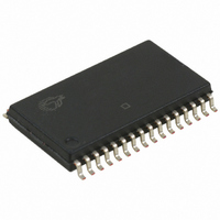
CY7C53120E2-10SXIT Cypress Semiconductor Corp, CY7C53120E2-10SXIT Datasheet - Page 5

CY7C53120E2-10SXIT
Manufacturer Part Number
CY7C53120E2-10SXIT
Description
IC PROCESSOR NEURON 32-SOIC
Manufacturer
Cypress Semiconductor Corp
Series
Neuron®r
Datasheet
1.CY7C53120E2-10SXIT.pdf
(14 pages)
Specifications of CY7C53120E2-10SXIT
Applications
Network Processor
Core Processor
Pipelined
Program Memory Type
FLASH (2 kB), ROM (10 kB)
Controller Series
CY7C531xx
Ram Size
2K x 8
Interface
Serial
Number Of I /o
11
Voltage - Supply
4.5 V ~ 5.5 V
Operating Temperature
-40°C ~ 85°C
Mounting Type
Surface Mount
Package / Case
32-SOIC (11.30mm Width)
Lead Free Status / RoHS Status
Lead free / RoHS Compliant
Document #: 38-10001 Rev. *E
Memory Usage
All Neuron chips require system firmware to be present when
they are powered up. In the case of the CY7C53120 family,
this firmware is preprogrammed in the factory in an on-chip
ROM. In the case of the CY7C53150, the system firmware
must be present in the first 16 KB of an off-chip nonvolatile
memory such as Flash, EPROM, EEPROM, or NVRAM.
These devices must be programmed in a device programmer
before board assembly. Because the system firmware imple-
ments the network protocol, it cannot itself be downloaded
over the network.
For the CY7C53120 family, the user application program is
stored in on-chip Flash memory. It may be programmed using
a device programmer before board assembly, or may be
downloaded and updated over the LonTalk network from an
external network management tool.
For the CY7C53150, the user application program is stored in
on-chip Flash Memory and also in off-chip memory. The user
program may initially be programmed into the off-chip memory
device using a device programmer.
Flash Memory Retention and Endurance
Data and code stored in Flash Memory is guaranteed to be
retained for at least 10 years for programming temperature
range of –25°C to 85°C.
The Flash Memory can typically be written 100,000 times
without any data loss.
system firmware extends the effective endurance of Flash
memory in two ways. If the data being written to a byte of Flash
memory is the same as the data already present in that byte,
the firmware does not perform the physical write. So for
example, an application that sets its own address in Flash
memory after every reset does not use up any write cycles if
the address has not changed. In addition, system firmware
version 13.1 or higher is able to aggregate writes to eight
successive address locations into a single write for
CY7C53120E4 devices. For example, if 4 KB of code is
downloaded over the network, the firmware would execute
only 512 writes rather than 4,096.
Note
5. For detailed information about data retention after 100K cycles, see the Cypress qualification report.
[5]
An erase/write cycle takes 20 ms. The
40 MHz 3120 Operation
The CY7C53120E4-40 device was designed to run at
frequencies up to 40 MHz using an external clock oscillator. It
is important to note that external oscillators may typically take
on the order of 5 ms to stabilize after power-up. The Neuron
chip must be held in reset until the CLK1 input is stable. With
some oscillators, this may require the use of a reset-stretching
Low-Voltage Detection chip/circuit. Check the oscillator
vendor’s specification for more information about start-up
stabilization times.
Low-Voltage Inhibit Operation
The on-chip Low-voltage Inhibit circuit trips the Neuron chip
whenever the V
prevents the corruption of nonvolatile memory during voltage
drops.
Communications Port
The Neuron chip includes a versatile 5-pin communications
port that can be configured in three different ways. In
Single-Ended Mode, pin CP0 is used for receiving serial data,
pin CP1 for transmitting serial data, and pin CP2 enables an
external transceiver. Data is communicated using Differential
Manchester encoding.
In Special Purpose Mode, pin CP0 is used for receiving serial
data, pin CP1 for transmitting serial data, pin CP2 transmits a
bit clock, and pin CP4 transmits a frame clock for use by an
external intelligent transceiver. In this mode, the external
transceiver is responsible for encoding and decoding the data
stream.
In Differential Mode, pins CP0 and CP1 form a differential
receiver with built-in programmable hysteresis and low pass
filtering. Pins CP2 and CP3 form a differential driver. Serial
data is communicated using Differential Manchester encoding.
The following tables describe the communications port when
used in Differential Mode.
DD
input is less than 4.1 ± 0.3V. This feature
CY7C53150
CY7C53120
Page 5 of 14
[+] Feedback


