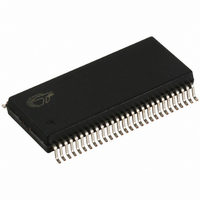
CY7C66113-PVC Cypress Semiconductor Corp, CY7C66113-PVC Datasheet - Page 27

CY7C66113-PVC
Manufacturer Part Number
CY7C66113-PVC
Description
IC MCU 8K USB HUB 4 PORT 56TSSOP
Manufacturer
Cypress Semiconductor Corp
Specifications of CY7C66113-PVC
Applications
USB Hub/Microcontroller
Core Processor
M8
Program Memory Type
OTP (8 kB)
Controller Series
USB Hub
Ram Size
256 x 8
Interface
I²C, USB, HAPI
Number Of I /o
31
Voltage - Supply
4 V ~ 5.5 V
Operating Temperature
0°C ~ 70°C
Mounting Type
Surface Mount
Package / Case
56-SSOP
Operating Temperature (max)
70C
Operating Temperature (min)
0C
Operating Temperature Classification
Commercial
Mounting
Surface Mount
Pin Count
56
Lead Free Status / RoHS Status
Contains lead / RoHS non-compliant
For Use With
CY3649 - PROGRAMMER HI-LO USB M8428-1339 - KIT LOW SPEED PERSONALITY BOARD
Lead Free Status / RoHS Status
Not Compliant, Contains lead / RoHS non-compliant
Other names
428-1330
Available stocks
Company
Part Number
Manufacturer
Quantity
Price
Company:
Part Number:
CY7C66113-PVC
Manufacturer:
CY
Quantity:
10
Bit 2 : ARB Lost/Restart
Bit 1 : Receive Stop
Bit 0 : I
14.0
The CY7C66x13 processor provides a hardware assisted parallel interface for bus widths of 8, 16, or 24 bits, to accommodate
data transfer with an external microcontroller or similar device. Control bits for selecting the byte width are in the HAPI/I
Configuration Register (Figure 12-1), bits 1 and 0.
Signals are provided on Port 2 to control the HAPI interface. Table 14-1 describes these signals and the HAPI control bits in the
HAPI/I
overridden. The Port 2 output pins are in CMOS output mode and Port 2 input pins are in input mode (open drain mode with Q3
OFF in Figure 9-1).
Table 14-1. Port 2 Pin and HAPI Configuration Bit Definitions
HAPI Read by External Device from CY7C66x13:
In this case (see Figure 25-3), firmware writes data to the GPIO ports. If 16-bit or 24-bit transfers are being made, Port 0 should
be written last, since writes to Port 0 asserts the Data Ready bit and the DReadyPin to signal the external device that data is
available.
The external device then drives the OE and CS pins active (LOW), which causes the HAPI data to be output on the port pins.
When OE is returned HIGH (inactive), the HAPI/GPIO interrupt is generated. At that point, firmware can reload the HAPI latches
for the next output, again writing Port 0 last.
The Data Ready bit reads the opposite state from the external DReadyPin on pin P2[3]. If the DRDY Polarity bit is 0, DReadyPin
is active HIGH, and the Data Ready bit is active LOW.
HAPI Write by External Device to CY7C66x13:
Document #: 38-08024 Rev. *A
Pin
P2[2]
P2[3]
P2[4]
P2[5]
P2[6]
Bit
2
3
4
5
This bit is set by the I
The Addr bit is cleared when the firmware sets the Continue bit. This bit allows the firmware to recognize when the master
has lost arbitration, and in slave mode it allows the firmware to recognize that a start or restart has occurred.
This bit is valid as a status bit (ARB Lost) after master mode transactions. In master mode, set this bit (along with the
Continue and MSTR Mode bits) to perform an I
to the data register before setting the Continue bit. To prevent false ARB Lost signals, the Restart bit is cleared by hardware
during the restart sequence.
This bit is set when the slave is in receive mode and detects a stop bit on the bus. The Receive Stop bit is not set if the
firmware terminates the I
e.g. in receive mode if firmware sets the Continue bit and clears the ACK bit.
Set this bit to override GPIO definition with I
these pins are free to function as GPIOs. In I
of the GPIO configuration setting.
2
2
C Configuration Register. Enabling HAPI causes the GPIO setting in the GPIO Configuration Register (Figure 9-6) to be
C Enable
Hardware Assisted Parallel Interface (HAPI)
Name
LatEmptyPin
DReadyPin
STB
OE
CS
Name
Data Ready
Latch Empty
DRDY Polarity
LEMPTY Polarity
2
C-compatible block during the first byte of a slave receive transaction, after an I
2
C transaction by not acknowledging the previous byte transmitted on the I
Direction
Out
Out
In
In
In
R/W
R
R
R/W
R/W
Description (Port 2 Pin)
Ready for more input data from external interface.
Output data ready for external interface.
Strobe signal for latching incoming data.
Output Enable, causes chip to output data.
Chip Select (Gates STB and OE).
Description (HAPI/I
Asserted after firmware writes data to Port 0, until OE driven LOW.
Asserted after firmware reads data from Port 0, until STB driven LOW.
Determines polarity of Data Ready bit and DReadyPin:
If 0, Data Ready is active LOW, DReadyPin is active HIGH.
If 1, Data Ready is active HIGH, DReadyPin is active LOW.
Determines polarity of Latch Empty bit and LatEmptyPin:
If 0, Latch Empty is active LOW, LatEmptyPin is active HIGH.
If 1, Latch Empty is active HIGH, LatEmptyPin is active LOW.
2
C-compatible function on the two I
2
C-compatible mode, the two pins operate in open drain mode, independent
2
C restart sequence. The I
2
C Configuration Register)
2
C target address for the restart must be written
2
C-compatible pins. When this bit is cleared,
2
CY7C66013
CY7C66113
C-compatible bus,
2
C start or restart.
Page 27 of 58
2
C


