CY7C66113-PVC Cypress Semiconductor Corp, CY7C66113-PVC Datasheet - Page 21
CY7C66113-PVC
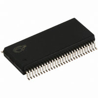
Manufacturer Part Number
CY7C66113-PVC
Description
IC MCU 8K USB HUB 4 PORT 56TSSOP
Manufacturer
Cypress Semiconductor Corp
Specifications of CY7C66113-PVC
Applications
USB Hub/Microcontroller
Core Processor
M8
Program Memory Type
OTP (8 kB)
Controller Series
USB Hub
Ram Size
256 x 8
Interface
I²C, USB, HAPI
Number Of I /o
31
Voltage - Supply
4 V ~ 5.5 V
Operating Temperature
0°C ~ 70°C
Mounting Type
Surface Mount
Package / Case
56-SSOP
Operating Temperature (max)
70C
Operating Temperature (min)
0C
Operating Temperature Classification
Commercial
Mounting
Surface Mount
Pin Count
56
Lead Free Status / RoHS Status
Contains lead / RoHS non-compliant
For Use With
CY3649 - PROGRAMMER HI-LO USB M8428-1339 - KIT LOW SPEED PERSONALITY BOARD
Lead Free Status / RoHS Status
Not Compliant, Contains lead / RoHS non-compliant
Other names
428-1330
Available stocks
Company
Part Number
Manufacturer
Quantity
Price
Company:

Part Number:
CY7C66113-PVC
Manufacturer:
CY
Quantity:
10


As shown in Table 9-1 below, a positive polarity on an input pin represents a rising edge interrupt (LOW to HIGH), and a negative
polarity on an input pin represents a falling edge interrupt (HIGH to LOW).
The GPIO interrupt is generated when all of the following conditions are met: the Interrupt Enable bit of the associated Port
Interrupt Enable Register is enabled, the GPIO Interrupt Enable bit of the Global Interrupt Enable Register (Figure 16-1) is
enabled, the Interrupt Enable Sense (bit 2, Figure 15-1) is set, and the GPIO pin of the port sees an event matching the interrupt
polarity.
The driving state of each GPIO pin is determined by the value written to the pin’s Data Register (Figure 9-2 through Figure 9-5)
and by its associated Port Configuration bits as shown in the GPIO Configuration Register (Figure 9-6). These ports are
configured on a per-port basis, so all pins in a given port are configured together. The possible port configurations are detailed
in Table 9-1. As shown in this table below, when a GPIO port is configured with CMOS outputs, interrupts from that port are
disabled.
During reset, all of the bits in the GPIO Configuration Register are written with ‘0’ to select Hi-Z mode for all GPIO ports as the
default configuration.
Table 9-1. GPIO Port Output Control Truth Table and Interrupt Polarity
Q1, Q2, and Q3 discussed below are the transistors referenced in Figure 9-1. The available GPIO drive strength are:
9.2
Each GPIO pin can be individually enabled or disabled as an interrupt source. The Port 0–3 Interrupt Enable registers provide
this feature with an interrupt enable bit for each GPIO pin. When HAPI mode (Section 14.0) is enabled the GPIO interrupts are
blocked, including ports not used by HAPI, so GPIO pins cannot be used as interrupt sources.
During a reset, GPIO interrupts are disabled by clearing all of the GPIO interrupt enable ports. Writing a ‘1’ to a GPIO Interrupt
Enable bit enables GPIO interrupts from the corresponding input pin. All GPIO pins share a common interrupt, as discussed in
Section 16.8.
Port 0 Interrupt Enable
Document #: 38-08024 Rev. *A
Bit #
Bit Name
Read/Write
Reset
Port Config Bit 1 Port Config Bit 0 Data Register Output Drive Strength Interrupt Enable Bit
• Output LOW Mode: The pin’s Data Register is set to ‘0’
• Output HIGH Mode: The pin’s Data Register is set to 1 and the Port Configuration Bits[1:0] is set to ‘10’
• Resistive Mode: The pin’s Data Register is set to 1 and the Port Configuration Bits[1:0] is set to ‘11’
• Hi-Z Mode: The pin’s Data Register is set to1 and Port Configuration Bits[1:0] is set either ‘00’ or ‘01’
Writing ‘0’ to the pin’s Data Register puts the pin in output LOW mode, regardless of the contents of the Port Configuration
Bits[1:0]. In this mode, Q1 and Q2 are OFF. Q3 is ON. The GPIO pin is driven LOW through Q3.
In this mode, Q1 and Q3 are OFF. Q2 is ON. The GPIO is pulled up through Q2. The GPIO pin is capable of sourcing ... of
current.
Q2 and Q3 are OFF. Q1 is ON. The GPIO pin is pulled up with an internal 14k resistor. In resistive mode, the pin may serve
as an input. Reading the pin’s Data Register returns a logic HIGH if the pin is not driven LOW by an external source.
Q1, Q2, and Q3 are all OFF. The GPIO pin is not driven internally. In this mode, the pin may serve as an input. Reading the
Port Data Register returns the actual logic value on the port pins.
1
1
0
0
GPIO Interrupt Enable Ports
7
P0.7 Intr
Enable
W
0
1
0
1
0
6
P0.6 Intr
Enable
W
0
5
P0.5 Intr
Enable
W
0
0
1
0
1
0
1
0
1
Figure 9-7. Port 0 Interrupt Enable
Output LOW
Resistive
Output LOW
Output HIGH
Output LOW
Hi-Z
Output LOW
Hi-Z
4
P0.4 Intr
Enable
W
0
3
P0.3 Intr
Enable
W
0
2
P0.2 Intr
Enable
W
0
0
1
0
1
0
1
0
1
1
P0.1 Intr
Enable
W
0
Disabled
– (Falling Edge)
Disabled
Disabled
Disabled
– (Falling Edge)
Disabled
+ (Rising Edge)
Interrupt Polarity
CY7C66013
CY7C66113
Page 21 of 58
ADDRESS 0x04
0
P0.0 Intr
Enable
W
0
Related parts for CY7C66113-PVC
Image
Part Number
Description
Manufacturer
Datasheet
Request
R

Part Number:
Description:
Manufacturer:
Cypress Semiconductor Corp
Datasheet:
Part Number:
Description:
Manufacturer:
Cypress Semiconductor Corp
Datasheet:
Part Number:
Description:
Manufacturer:
Cypress Semiconductor Corp
Datasheet:
Part Number:
Description:
Manufacturer:
Cypress Semiconductor Corp
Datasheet:
Part Number:
Description:
Manufacturer:
Cypress Semiconductor Corp
Datasheet: