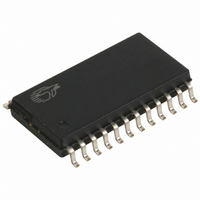
CY7C63613-SC Cypress Semiconductor Corp, CY7C63613-SC Datasheet - Page 17

CY7C63613-SC
Manufacturer Part Number
CY7C63613-SC
Description
IC MCU 8K USB LS MCU 24-SOIC
Manufacturer
Cypress Semiconductor Corp
Series
M8™r
Datasheet
1.CY7C63613-SC.pdf
(30 pages)
Specifications of CY7C63613-SC
Applications
USB Microcontroller
Core Processor
M8B
Program Memory Type
OTP (8 kB)
Controller Series
CY7C636xx
Ram Size
256 x 8
Interface
PS2, USB
Number Of I /o
16
Voltage - Supply
4 V ~ 5.5 V
Operating Temperature
0°C ~ 70°C
Mounting Type
Surface Mount
Package / Case
24-SOIC (7.5mm Width)
Lead Free Status / RoHS Status
Contains lead / RoHS non-compliant
Other names
428-1321
Available stocks
Company
Part Number
Manufacturer
Quantity
Price
Company:
Part Number:
CY7C63613-SC
Manufacturer:
CYP
Quantity:
5 510
Part Number:
CY7C63613-SC
Manufacturer:
CYPRESS/赛普拉斯
Quantity:
20 000
9.2
Every GPIO port can be programmed as inputs with internal pull-ups, open drain outputs, and traditional CMOS outputs. In ad-
dition, the interrupt polarity for each port can be programmed. With positive interrupt polarity, a rising edge (“0” to “1”) on an input
pin causes an interrupt. With negative polarity, a falling edge (“1” to “0”) on an input pin causes an interrupt. As shown in the table
below, when a GPIO port is configured with CMOS outputs, interrupts from that port are disabled. The GPIO Configuration Port
register provides two bits per port to program these features. The possible port configurations are:
In “Resistive” mode, a 7-k pull-up resistor is conditionally enabled for all pins of a GPIO port. The resistor is enabled for any pin
that has been written as a “1.” The resistor is disabled on any pin that has been written as a “0”. An I/O pin will be driven high
through a 7-k
abled, when a “0” has been written to the pin. An I/O pin that has been written as a “1” can be used as an input pin with an inte-
grated 7-k
interrupt enabled.
In “CMOS” mode, all pins of the GPIO port are outputs that are actively driven. The current source and sink capacity are roughly
the same (symmetric output drive). A CMOS port is not a possible source for interrupts.
A port configured in CMOS mode has interrupt generation disabled, yet the interrupt mask bits serve to control port direction. If
a port’s associated Interrupt Mask bits are cleared, those port bits are strictly outputs. If the Interrupt Mask bits are set then those
bits will be open drain inputs. As open drain inputs, if their data output values are ‘1’ those port pins will be CMOS inputs (HIGH
Z output).
In “Open Drain” mode the internal pull-up resistor and CMOS driver (HIGH) are both disabled. An I/O pin that has been written
as a “1” can be used as either a high-impedance input or a three-state output. An I/O pin that has been written as a “0” will drive
the output LOW. The interrupt polarity for an open drain GPIO port can be selected as either positive (rising edge) or negative
(falling edge).
During reset, all of the bits in the GPIO Configuration Register are written with “0”. This selects the default configuration: Open
Drain output, positive interrupt polarity for all GPIO ports.
10.0
The SIE allows the microcontroller to communicate with the USB host. The SIE simplifies the interface between the microcontroller
and USB by incorporating hardware that handles the following USB bus activity independently of the microcontroller:
Firmware is required to handle the rest of the USB interface with the following tasks:
• Bit stuffing/unstuffing
• Checksum generation/checking
• ACK/NAK
• Token type identification
• Address checking
• Coordinate enumeration by responding to set-up packets
• Fill and empty the FIFOs
• Suspend/Resume coordination
• Verify and select Data toggle values
Config Bit 1
Port Configuration bits
Port 3
7
GPIO Configuration Port
USB Serial Interface Engine (SIE)
pull-up resistor. Resistive mode selects a negative (falling edge) interrupt polarity on all pins that have the GPIO
11
10
10
01
00
pull-up resistor when a “1” has been written to the pin. Or the output pin will be driven LOW, with the pull-up dis-
Config Bit 0
Port 3
6
Figure 9-11. GPIO Configuration Register 0x08h (write only)
Config Bit 1
Port 2
5
Pin Interrupt Bit
PRELIMINARY
X
X
X
0
1
Config Bit 0
Port 2
4
17
Config Bit 1
Port 1
3
CMOS Output
Driver Mode
Open Drain
Open Drain
Open Drain
Resistive
Config Bit 0
Port 1
2
Config Bit 1
Port 0
Interrupt Polarity
1
CY7C63612/13
+ (default)
disabled
disabled
-
-
Config Bit 0
Port 0
0


