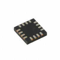
CY8CTMG200-16LGXI Cypress Semiconductor Corp, CY8CTMG200-16LGXI Datasheet - Page 31

CY8CTMG200-16LGXI
Manufacturer Part Number
CY8CTMG200-16LGXI
Description
IC MCU 32K FLASH 16-COL
Manufacturer
Cypress Semiconductor Corp
Series
TrueTouch™r
Datasheet
1.CY8CTST200-16LGXI.pdf
(308 pages)
Specifications of CY8CTMG200-16LGXI
Applications
Touchscreen Controller
Core Processor
M8C
Program Memory Type
FLASH (32 kB)
Controller Series
CY8CT
Ram Size
2K x 8
Interface
I²C, SPI, UART/USART, USB
Number Of I /o
13
Voltage - Supply
1.8 V
Operating Temperature
-40°C ~ 85°C
Mounting Type
Surface Mount
Package / Case
16-QFN
Processor Series
CY8CTxx2xx
Core
M8C
Data Bus Width
8 bit
For Use With
770-1000 - ISP 4PORT FOR CYPRESS PSOC MCU
Lead Free Status / RoHS Status
Lead free / RoHS Compliant
Other names
428-2952
Available stocks
Company
Part Number
Manufacturer
Quantity
Price
Company:
Part Number:
CY8CTMG200-16LGXI
Manufacturer:
CY
Quantity:
490
- Current page: 31 of 308
- Download datasheet (3Mb)
2.5.3
The three-byte instruction formats are the second most
prevalent instruction formats. These instructions need three
bytes because they either move data between two
addresses in the user accessible address space (registers
and RAM) or they hold 16-bit absolute addresses as the
destination of a long jump or long call.
Table 2-5. Three-Byte Instruction Formats
The first instruction format, shown in the first row of
Table
These instructions change program execution uncondition-
ally to an absolute address. The instructions use an 8-bit
opcode, leaving room for a 16-bit destination address.
PSoC CY8CTMG20x and CY8CTST200 TRM, Document No. 001-53603 Rev. *C
8-Bit Opcode
8-Bit Opcode
8-Bit Opcode
2-5,
Byte 0
is used by the LJMP and LCALL instructions.
Three-Byte Instructions
16-Bit Address (MSB, LSB)
8-Bit Address
8-Bit Address
Byte 1
8-Bit Data
8-Bit Address
Byte 2
The second three-byte instruction format, shown in the sec-
ond row of
ing modes:
■
■
The third three-byte instruction format, shown in the third
row of
addressing mode, which is used by only one instruction.
This instruction format uses an 8-bit opcode followed by two
8-bit addresses. The first address is the destination address
in RAM, while the second address is the source address in
RAM. The following is an example of this instruction:
MOV [7], [5]
Destination Direct Source Immediate (ADD [7], 5)
Destination Indexed Source Immediate
(ADD [X+7], 5)
Table
Table
2-5,
2-5,
is for the Destination Direct Source Direct
is used by the following two address-
CPU Core (M8C)
[+] Feedback
31
Related parts for CY8CTMG200-16LGXI
Image
Part Number
Description
Manufacturer
Datasheet
Request
R
Part Number:
Description:
CY8CTMG200-32LQXIT
Manufacturer:
Cypress Semiconductor Corp
Datasheet:

Part Number:
Description:
IC MCU 32K FLASH 24UQFN
Manufacturer:
Cypress Semiconductor Corp
Datasheet:

Part Number:
Description:
IC MCU 32K FLASH 32UQFN
Manufacturer:
Cypress Semiconductor Corp
Datasheet:

Part Number:
Description:
IC MCU 32K FLASH 48-QFN
Manufacturer:
Cypress Semiconductor Corp
Datasheet:
Part Number:
Description:
IC MCU 32K FLASH 16-COL
Manufacturer:
Cypress Semiconductor Corp
Datasheet:
Part Number:
Description:
IC MCU 32K FLASH 24UQFN
Manufacturer:
Cypress Semiconductor Corp
Datasheet:
Part Number:
Description:
IC MCU 32K FLASH 48-QFN
Manufacturer:
Cypress Semiconductor Corp
Datasheet:
Part Number:
Description:
Manufacturer:
Cypress Semiconductor Corp
Datasheet:
Part Number:
Description:
Manufacturer:
Cypress Semiconductor Corp
Datasheet:


