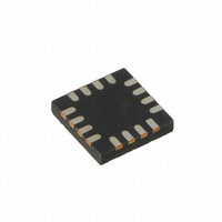
CY8CTMG200-16LGXI Cypress Semiconductor Corp, CY8CTMG200-16LGXI Datasheet - Page 153

CY8CTMG200-16LGXI
Manufacturer Part Number
CY8CTMG200-16LGXI
Description
IC MCU 32K FLASH 16-COL
Manufacturer
Cypress Semiconductor Corp
Series
TrueTouch™r
Datasheet
1.CY8CTST200-16LGXI.pdf
(308 pages)
Specifications of CY8CTMG200-16LGXI
Applications
Touchscreen Controller
Core Processor
M8C
Program Memory Type
FLASH (32 kB)
Controller Series
CY8CT
Ram Size
2K x 8
Interface
I²C, SPI, UART/USART, USB
Number Of I /o
13
Voltage - Supply
1.8 V
Operating Temperature
-40°C ~ 85°C
Mounting Type
Surface Mount
Package / Case
16-QFN
Processor Series
CY8CTxx2xx
Core
M8C
Data Bus Width
8 bit
For Use With
770-1000 - ISP 4PORT FOR CYPRESS PSOC MCU
Lead Free Status / RoHS Status
Lead free / RoHS Compliant
Other names
428-2952
Available stocks
Company
Part Number
Manufacturer
Quantity
Price
Company:
Part Number:
CY8CTMG200-16LGXI
Manufacturer:
CY
Quantity:
490
- Current page: 153 of 308
- Download datasheet (3Mb)
Normal Operation. Typical timing for an SPIM transfer is
shown in
writes a byte to transmit when TX Reg Empty status is true.
If no transmission is currently in progress, the data is loaded
into the shifter and the transmission is initiated. The TX Reg
Empty status is asserted again and the user is allowed to
write the next byte to be transmitted to the TX Buffer regis-
ter.
PSoC CY8CTMG20x and CY8CTST200 TRM, Document No. 001-53603 Rev. *C
Figure 18-5
INTERNAL CLOCK
clock is CLK input
internal bit rate
divided by two.
Free running,
TX REG EMPTY
SCLK (MODE 0)
SCLK (MODE 1)
RX REG FULL
CLK INPUT
User writes first
Buffer register.
byte to the TX
and
MOSI
Figure
18-6. The user initially
Buffer write.
Setup time
Figure 18-5. Typical SPIM Timing in Mode 0 and 1
for TX
First input bit
is latched.
D7
Shifter is loaded
with first byte.
First shift.
D6
After the last bit is output, if TX Buffer data is available with
one-half clock setup time to the next clock, a new byte trans-
mission is initiated. An SPIM block receives a byte at the
same time that it sends one. The SPI Complete or RX Reg
Full can be used to determine when the input byte has been
received.
User writes next
Buffer register.
D5
byte to the TX
edge and is latched
data is valid on this
Last bit of received
into RX Buffer.
D2
D1
D0
Shifter is loaded
with next byte.
D7
153
SPI
[+] Feedback
Related parts for CY8CTMG200-16LGXI
Image
Part Number
Description
Manufacturer
Datasheet
Request
R
Part Number:
Description:
CY8CTMG200-32LQXIT
Manufacturer:
Cypress Semiconductor Corp
Datasheet:

Part Number:
Description:
IC MCU 32K FLASH 24UQFN
Manufacturer:
Cypress Semiconductor Corp
Datasheet:

Part Number:
Description:
IC MCU 32K FLASH 32UQFN
Manufacturer:
Cypress Semiconductor Corp
Datasheet:

Part Number:
Description:
IC MCU 32K FLASH 48-QFN
Manufacturer:
Cypress Semiconductor Corp
Datasheet:
Part Number:
Description:
IC MCU 32K FLASH 16-COL
Manufacturer:
Cypress Semiconductor Corp
Datasheet:
Part Number:
Description:
IC MCU 32K FLASH 24UQFN
Manufacturer:
Cypress Semiconductor Corp
Datasheet:
Part Number:
Description:
IC MCU 32K FLASH 48-QFN
Manufacturer:
Cypress Semiconductor Corp
Datasheet:
Part Number:
Description:
Manufacturer:
Cypress Semiconductor Corp
Datasheet:
Part Number:
Description:
Manufacturer:
Cypress Semiconductor Corp
Datasheet:


