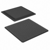
XC3S1400AN-4FGG676I Xilinx Inc, XC3S1400AN-4FGG676I Datasheet - Page 67

XC3S1400AN-4FGG676I
Manufacturer Part Number
XC3S1400AN-4FGG676I
Description
IC FPGA SPARTAN-AN 1400K 676FBGA
Manufacturer
Xilinx Inc
Series
Spartan™-3ANr
Datasheets
1.XC3S50A-4VQG100C.pdf
(7 pages)
2.XC3S50AN-4TQG144C.pdf
(2 pages)
3.XC3S50AN-4TQG144C.pdf
(123 pages)
Specifications of XC3S1400AN-4FGG676I
Total Ram Bits
589824
Number Of Logic Elements/cells
25344
Number Of Labs/clbs
2816
Number Of I /o
502
Number Of Gates
1400000
Voltage - Supply
1.14 V ~ 1.26 V
Mounting Type
Surface Mount
Operating Temperature
-40°C ~ 100°C
Package / Case
676-BBGA
No. Of Logic Blocks
2816
No. Of Gates
1400000
No. Of Macrocells
25344
Family Type
Spartan-3AN
No. Of Speed Grades
4
No. Of I/o's
502
Clock
RoHS Compliant
Lead Free Status / RoHS Status
Lead free / RoHS Compliant
Available stocks
Company
Part Number
Manufacturer
Quantity
Price
Company:
Part Number:
XC3S1400AN-4FGG676I
Manufacturer:
PANASONIC
Quantity:
10 000
Company:
Part Number:
XC3S1400AN-4FGG676I
Manufacturer:
Xilinx Inc
Quantity:
10 000
Company:
Part Number:
XC3S1400AN-4FGG676I/XC3S1400AN-5FGG676C
Manufacturer:
XILINX
0
Table 59: Timing for Byte-wide Peripheral Interface (BPI) Configuration Mode
Table 60: Configuration Timing Requirements for Attached Parallel NOR Flash
IEEE 1149.1/1532 JTAG Test Access Port Timing
X-Ref Target - Figure 18
DS557 (v4.1) April 1, 2011
Product Specification
Notes:
1.
2.
3.
T
T
T
T
T
T
T
T
T
(t
T
(t
T
(t
T
(t
ACC
CCLK1
CCLKn
MINIT
INITM
INITADDR
CCO
DCC
CCD
CE
ELQV
OE
GLQV
AVQV
BYTE
FLQV,
Symbol
Symbol
These requirements are for successful FPGA configuration in BPI mode, where the FPGA generates the CCLK signal. The
post-configuration timing can be different to support the specific needs of the application loaded into the FPGA.
Subtract additional printed circuit board routing delay as required by the application.
The initial BYTE# timing can be extended using an external, appropriately sized pull-down resistor on the FPGA’s LDC2 pin. The resistor
value also depends on whether the FPGA’s PUDC_B pin is High or Low.
)
)
)
t
FHQV
TCK
TMS
TDI
TDO
(Input)
(Input)
(Input)
(Output)
)
Initial CCLK clock period
CCLK clock period after FPGA loads ConfigRate setting
Setup time on M[2:0] mode pins before the rising edge of INIT_B
Hold time on M[2:0] mode pins after the rising edge of INIT_B
Minimum period of initial A[25:0] address cycle; LDC[2:0] and HDC are asserted
and valid
Address A[25:0] outputs valid after CCLK falling edge
Setup time on D[7:0] data inputs before CCLK rising edge
Hold time on D[7:0] data inputs after CCLK rising edge
Parallel NOR Flash PROM chip-select time
Parallel NOR Flash PROM output-enable time
Parallel NOR Flash PROM read access time
For x8/x16 PROMs only: BYTE# to output valid time
Description
T
TDITCK
T
TMSTCK
Description
Figure 18: JTAG Waveforms
www.xilinx.com
Spartan-3AN FPGA Family: DC and Switching Characteristics
T
TCKTDI
T
TCKTMS
(3)
T
ACC
T
0.5T
TCKTDO
T
CCLKn min
T
T
BYTE
CE
OE
Requirement
T
CCH
T
Minimum
T
T
INITADDR
INITADDR
1/F
INITADDR
–
50
0
0
5
TCK
T
See T
CCO
T
See
See
See
SMDCC
CCL
–
Maximum
T
Table 51
Table 51
Table 55
DCC
DS557_13_083110
in
–
–
5
–
Table 56
–
PCB
T
cycles
Units
CCLK1
Units
ns
ns
ns
ns
ns
ns
ns
67


