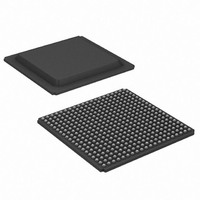
XA3S400A-4FGG400Q Xilinx Inc, XA3S400A-4FGG400Q Datasheet - Page 38

XA3S400A-4FGG400Q
Manufacturer Part Number
XA3S400A-4FGG400Q
Description
IC FPGA SPARTAN-3A 400K 400-FBGA
Manufacturer
Xilinx Inc
Series
Spartan™-3A XAr
Datasheet
1.XA3S200A-4FTG256I.pdf
(56 pages)
Specifications of XA3S400A-4FGG400Q
Number Of Logic Elements/cells
8064
Number Of Labs/clbs
896
Total Ram Bits
368640
Number Of I /o
311
Number Of Gates
400000
Voltage - Supply
1.14 V ~ 1.26 V
Mounting Type
Surface Mount
Operating Temperature
-40°C ~ 125°C
Package / Case
400-BGA
Lead Free Status / RoHS Status
Lead free / RoHS Compliant
Available stocks
Company
Part Number
Manufacturer
Quantity
Price
Company:
Part Number:
XA3S400A-4FGG400Q
Manufacturer:
XilinxInc
Quantity:
3 000
Company:
Part Number:
XA3S400A-4FGG400Q
Manufacturer:
Xilinx Inc
Quantity:
10 000
Part Number:
XA3S400A-4FGG400Q
Manufacturer:
XILINX/赛灵思
Quantity:
20 000
Table 33: 18 x 18 Embedded Multiplier Timing (Continued)
Block RAM Timing
Table 34: Block RAM Timing
38
Notes:
1.
2.
3.
4.
5.
Notes:
1.
Clock Frequency
F
Clock-to-Output Times
T
Setup Times
T
T
T
T
Hold Times
T
T
T
T
Clock Timing
T
T
Clock Frequency
F
MULT
RCKO
RCCK_ADDR
RDCK_DIB
RCCK_ENB
RCCK_WEB
RCKC_ADDR
RCKD_DIB
RCKC_ENB
RCKC_WEB
BPWH
BPWL
BRAM
Symbol
Symbol
Combinational delay is less and pipelined performance is higher when multiplying input data with less than 18 bits.
The PREG register is typically used in both single-stage and two-stage pipelined multiplier implementations.
The PREG register is typically used when inferring a single-stage multiplier.
Input registers AREG or BREG are typically used when inferring a two-stage multiplier.
The numbers in this table are based on the operating conditions set forth in
The numbers in this table are based on the operating conditions set forth in
When reading from block RAM, the delay from the active transition at the CLK input
to data appearing at the DOUT output
Setup time for the ADDR inputs before the active transition at the CLK input of the
block RAM
Setup time for data at the DIN inputs before the active transition at the CLK input of
the block RAM
Setup time for the EN input before the active transition at the CLK input of the block
RAM
Setup time for the WE input before the active transition at the CLK input of the block
RAM
Hold time on the ADDR inputs after the active transition at the CLK input
Hold time on the DIN inputs after the active transition at the CLK input
Hold time on the EN input after the active transition at the CLK input
Hold time on the WE input after the active transition at the CLK input
High pulse width of the CLK signal
Low pulse width of the CLK signal
Block RAM clock frequency
Internal operating frequency for a two-stage 18x18 multiplier using the AREG and BREG
input registers and the PREG output register
Description
Description
www.xilinx.com
(1)
Table
Table
8.
8.
0.36
0.31
0.77
1.26
1.79
1.79
Min
Speed Grade
0
–
0
0
0
0
DS681 (v1.1) February 3, 2009
Min
Speed Grade
0
-4
Product Specification
-4
Max
2.49
280
–
–
–
–
–
–
–
–
–
–
Max
250
Units
MHz
ns
ns
ns
ns
ns
ns
ns
ns
ns
ns
ns
Units
MHz
R


