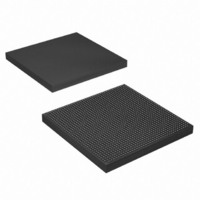
EP4SGX290KF40C3N Altera, EP4SGX290KF40C3N Datasheet - Page 290

EP4SGX290KF40C3N
Manufacturer Part Number
EP4SGX290KF40C3N
Description
IC STRATIX IV GX 290K 1517FBGA
Manufacturer
Altera
Series
Stratix® IV GXr
Datasheets
1.EP4SGX110DF29C3N.pdf
(80 pages)
2.EP4SGX110DF29C3N.pdf
(1154 pages)
3.EP4SGX110DF29C3N.pdf
(432 pages)
4.EP4SGX110DF29C3N.pdf
(22 pages)
5.EP4SGX110DF29C3N.pdf
(30 pages)
6.EP4SGX110DF29C3N.pdf
(72 pages)
Specifications of EP4SGX290KF40C3N
Number Of Logic Elements/cells
291200
Number Of Labs/clbs
11648
Total Ram Bits
17248
Number Of I /o
744
Voltage - Supply
0.87 V ~ 0.93 V
Mounting Type
Surface Mount
Operating Temperature
0°C ~ 85°C
Package / Case
1517-FBGA
Lead Free Status / RoHS Status
Lead free / RoHS Compliant
Number Of Gates
-
Other names
544-2624
Available stocks
Company
Part Number
Manufacturer
Quantity
Price
- EP4SGX110DF29C3N PDF datasheet
- EP4SGX110DF29C3N PDF datasheet #2
- EP4SGX110DF29C3N PDF datasheet #3
- EP4SGX110DF29C3N PDF datasheet #4
- EP4SGX110DF29C3N PDF datasheet #5
- EP4SGX110DF29C3N PDF datasheet #6
- Current page: 290 of 432
- Download datasheet (11Mb)
8–12
Stratix IV Device Handbook Volume 1
The load enable (LVDS_LOAD_EN) signal and the diffioclk signal (the clock running at
serial data rate) generated from PLL_Lx (left PLL) or PLL_Rx (right PLL) clocks the load
and shift registers. You can statically set the serialization factor to ×3, ×4, ×6, ×7, ×8, or
×10 using the Quartus II software. The load enable signal is derived from the
serialization factor setting.
transmitter.
Figure 8–5. Stratix IV Transmitter
Notes to
(1) In SDR and DDR modes, the data width is 1 and 2 bits, respectively.
(2) The tx_in port has a maximum data width of 10 bits.
You can configure any Stratix IV transmitter data channel to generate a
source-synchronous transmitter clock output. This flexibility allows the placement of
the output clock near the data outputs to simplify board layout and reduce
clock-to-data skew. Different applications often require specific clock-to-data
alignments or specific data-rate-to-clock-rate factors. The transmitter can output a
clock signal at the same rate as the data with a maximum frequency of 800 MHz. The
output clock can also be divided by a factor of 1, 2, 4, 6, 8, or 10, depending on the
serialization factor. You can set the phase of the clock in relation to the data at 0° or
180° (edge or center aligned). The left and right PLLs (PLL_Lx and PLL_Rx) provide
additional support for other phase shifts in 45° increments. These settings are made
statically in the Quartus II MegaWizard Plug-In Manager software.
tx_coreclock
Figure
Fabric
FPGA
tx_in 10
8–5:
Left/Right PLL
DIN
Serializer
3
DOUT
(LVDS_LOAD_EN, diffioclk, tx_coreclock)
Chapter 8: High-Speed Differential I/O Interfaces and DPA in Stratix IV Devices
Figure 8–5
2
(Note
IOE
1),
tx_inclock
shows a block diagram of the Stratix IV
(2)
LVDS Transmitter
IOE supports SDR, DDR, or
Non-Registered Datapath
February 2011 Altera Corporation
LVDS Clock Domain
Differential Transmitter
+
-
tx_out
Related parts for EP4SGX290KF40C3N
Image
Part Number
Description
Manufacturer
Datasheet
Request
R

Part Number:
Description:
CYCLONE II STARTER KIT EP2C20N
Manufacturer:
Altera
Datasheet:

Part Number:
Description:
CPLD, EP610 Family, ECMOS Process, 300 Gates, 16 Macro Cells, 16 Reg., 16 User I/Os, 5V Supply, 35 Speed Grade, 24DIP
Manufacturer:
Altera Corporation
Datasheet:

Part Number:
Description:
CPLD, EP610 Family, ECMOS Process, 300 Gates, 16 Macro Cells, 16 Reg., 16 User I/Os, 5V Supply, 15 Speed Grade, 24DIP
Manufacturer:
Altera Corporation
Datasheet:

Part Number:
Description:
Manufacturer:
Altera Corporation
Datasheet:

Part Number:
Description:
CPLD, EP610 Family, ECMOS Process, 300 Gates, 16 Macro Cells, 16 Reg., 16 User I/Os, 5V Supply, 30 Speed Grade, 24DIP
Manufacturer:
Altera Corporation
Datasheet:

Part Number:
Description:
High-performance, low-power erasable programmable logic devices with 8 macrocells, 10ns
Manufacturer:
Altera Corporation
Datasheet:

Part Number:
Description:
High-performance, low-power erasable programmable logic devices with 8 macrocells, 7ns
Manufacturer:
Altera Corporation
Datasheet:

Part Number:
Description:
Classic EPLD
Manufacturer:
Altera Corporation
Datasheet:

Part Number:
Description:
High-performance, low-power erasable programmable logic devices with 8 macrocells, 10ns
Manufacturer:
Altera Corporation
Datasheet:

Part Number:
Description:
Manufacturer:
Altera Corporation
Datasheet:

Part Number:
Description:
Manufacturer:
Altera Corporation
Datasheet:

Part Number:
Description:
Manufacturer:
Altera Corporation
Datasheet:

Part Number:
Description:
CPLD, EP610 Family, ECMOS Process, 300 Gates, 16 Macro Cells, 16 Reg., 16 User I/Os, 5V Supply, 25 Speed Grade, 24DIP
Manufacturer:
Altera Corporation
Datasheet:


