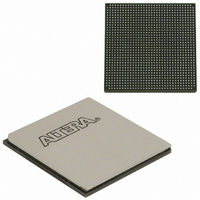
EP2SGX90EF1152C5N Altera, EP2SGX90EF1152C5N Datasheet - Page 43

EP2SGX90EF1152C5N
Manufacturer Part Number
EP2SGX90EF1152C5N
Description
IC STRATIX II GX 90K 1152-FBGA
Manufacturer
Altera
Series
Stratix® II GXr
Datasheet
1.EP2SGX30DF780C5.pdf
(316 pages)
Specifications of EP2SGX90EF1152C5N
Number Of Logic Elements/cells
90960
Number Of Labs/clbs
4548
Total Ram Bits
4520448
Number Of I /o
558
Voltage - Supply
1.15 V ~ 1.25 V
Mounting Type
Surface Mount
Operating Temperature
0°C ~ 70°C
Package / Case
1152-FBGA
For Use With
544-1725 - PCIE KIT W/S II GX EP2SGX90N544-1724 - SI KIT W/SII GX EP2SGX90N544-1702 - VIDEO KIT W/SII GX EP2SGX90N
Lead Free Status / RoHS Status
Lead free / RoHS Compliant
Number Of Gates
-
Other names
544-1768
EP2SGX90EF35C5NES
EP2SGX90EF35C5NES
Available stocks
Company
Part Number
Manufacturer
Quantity
Price
- Current page: 43 of 316
- Download datasheet (2Mb)
Altera Corporation
October 2007
Transceiver Clocking
Each Stratix II GX device transceiver block contains two transmitter PLLs
and four receiver PLLs. These PLLs can be driven by either of the two
reference clocks per transceiver block. These REFCLK signals can drive all
global clocks, transmitter PLL inputs, and all receiver PLL inputs.
Subsequently, the transmitter PLL output can only drive global clock
lines and the receiver PLL reference clock port. Only one of the two
reference clocks in a quad can drive the Inter Quad (I/Q) lines to clock the
PLLs in the other quads.
Figure 2–29
global clock connections for the EP2SGX130 device.
shows the inter-transceiver line connections as well as the
Stratix II GX Device Handbook, Volume 1
Stratix II GX Architecture
2–35
Related parts for EP2SGX90EF1152C5N
Image
Part Number
Description
Manufacturer
Datasheet
Request
R

Part Number:
Description:
CYCLONE II STARTER KIT EP2C20N
Manufacturer:
Altera
Datasheet:

Part Number:
Description:
CPLD, EP610 Family, ECMOS Process, 300 Gates, 16 Macro Cells, 16 Reg., 16 User I/Os, 5V Supply, 35 Speed Grade, 24DIP
Manufacturer:
Altera Corporation
Datasheet:

Part Number:
Description:
CPLD, EP610 Family, ECMOS Process, 300 Gates, 16 Macro Cells, 16 Reg., 16 User I/Os, 5V Supply, 15 Speed Grade, 24DIP
Manufacturer:
Altera Corporation
Datasheet:

Part Number:
Description:
Manufacturer:
Altera Corporation
Datasheet:

Part Number:
Description:
CPLD, EP610 Family, ECMOS Process, 300 Gates, 16 Macro Cells, 16 Reg., 16 User I/Os, 5V Supply, 30 Speed Grade, 24DIP
Manufacturer:
Altera Corporation
Datasheet:

Part Number:
Description:
High-performance, low-power erasable programmable logic devices with 8 macrocells, 10ns
Manufacturer:
Altera Corporation
Datasheet:

Part Number:
Description:
High-performance, low-power erasable programmable logic devices with 8 macrocells, 7ns
Manufacturer:
Altera Corporation
Datasheet:

Part Number:
Description:
Classic EPLD
Manufacturer:
Altera Corporation
Datasheet:

Part Number:
Description:
High-performance, low-power erasable programmable logic devices with 8 macrocells, 10ns
Manufacturer:
Altera Corporation
Datasheet:

Part Number:
Description:
Manufacturer:
Altera Corporation
Datasheet:

Part Number:
Description:
Manufacturer:
Altera Corporation
Datasheet:

Part Number:
Description:
Manufacturer:
Altera Corporation
Datasheet:

Part Number:
Description:
CPLD, EP610 Family, ECMOS Process, 300 Gates, 16 Macro Cells, 16 Reg., 16 User I/Os, 5V Supply, 25 Speed Grade, 24DIP
Manufacturer:
Altera Corporation
Datasheet:


