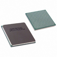
EP1S30F780I6 Altera, EP1S30F780I6 Datasheet - Page 142

EP1S30F780I6
Manufacturer Part Number
EP1S30F780I6
Description
IC STRATIX FPGA 30K LE 780-FBGA
Manufacturer
Altera
Series
Stratix®r
Datasheet
1.EP1S10F780C7.pdf
(276 pages)
Specifications of EP1S30F780I6
Number Of Logic Elements/cells
32470
Number Of Labs/clbs
3247
Total Ram Bits
3317184
Number Of I /o
597
Voltage - Supply
1.425 V ~ 1.575 V
Mounting Type
Surface Mount
Operating Temperature
-40°C ~ 100°C
Package / Case
780-FBGA
Family Name
Stratix
Number Of Logic Blocks/elements
32470
# I/os (max)
597
Frequency (max)
450.05MHz
Process Technology
0.13um (CMOS)
Operating Supply Voltage (typ)
1.5V
Logic Cells
32470
Ram Bits
3317184
Operating Supply Voltage (min)
1.425V
Operating Supply Voltage (max)
1.575V
Operating Temp Range
-40C to 100C
Operating Temperature Classification
Industrial
Mounting
Surface Mount
Pin Count
780
Package Type
FC-FBGA
Lead Free Status / RoHS Status
Contains lead / RoHS non-compliant
Number Of Gates
-
Lead Free Status / Rohs Status
Not Compliant
Other names
544-1861
EP1S30F780I6
EP1S30F780I6
Available stocks
Company
Part Number
Manufacturer
Quantity
Price
Company:
Part Number:
EP1S30F780I6N
Manufacturer:
ALTERA
Quantity:
996
- Current page: 142 of 276
- Download datasheet (4Mb)
I/O Structure
2–128
Stratix Device Handbook, Volume 1
Notes to
(1)
(2)
Differential termination (1),
Table 2–33. Differential Termination Supported by I/O Banks
Differential Termination Support
Clock pin CLK0, CLK2, CLK9, CLK11, and pins FPLL[7..10]CLK do not support differential termination.
Differential termination is only supported for LVDS because of a 3.3-V V
Table
2–33:
(2)
Figure 2–71. LVDS Input Differential On-Chip Termination
I/O banks on the left and right side of the device support LVDS receiver
(far-end) differential termination.
Table 2–33
Table 2–34
The differential on-chip resistance at the receiver input buffer is
118
Top and bottom I/O banks (3, 4, 7, and 8)
DIFFIO_RX[]
CLK[0,2,9,11],CLK[4-7],CLK[12-15]
CLK[1,3,8,10]
FCLK
FPLL[7..10]CLK
Table 2–34. Differential Termination Support Across Pin Types
Ω ±
20 %.
I/O Standard Support
Transmitting
shows the Stratix device differential termination support.
shows the termination support for different pin types.
Device
+
Ð
LVDS
Pin Type
Banks (3, 4, 7 & 8)
Z
Z
Top & Bottom
0
0
C C I O
.
Differential Termination
Receiving Device with
R
D
Left & Right Banks
Altera Corporation
(1, 2, 5 & 6)
+
Ð
v
R
v
v
July 2005
D
Related parts for EP1S30F780I6
Image
Part Number
Description
Manufacturer
Datasheet
Request
R

Part Number:
Description:
CYCLONE II STARTER KIT EP2C20N
Manufacturer:
Altera
Datasheet:

Part Number:
Description:
CPLD, EP610 Family, ECMOS Process, 300 Gates, 16 Macro Cells, 16 Reg., 16 User I/Os, 5V Supply, 35 Speed Grade, 24DIP
Manufacturer:
Altera Corporation
Datasheet:

Part Number:
Description:
CPLD, EP610 Family, ECMOS Process, 300 Gates, 16 Macro Cells, 16 Reg., 16 User I/Os, 5V Supply, 15 Speed Grade, 24DIP
Manufacturer:
Altera Corporation
Datasheet:

Part Number:
Description:
Manufacturer:
Altera Corporation
Datasheet:

Part Number:
Description:
CPLD, EP610 Family, ECMOS Process, 300 Gates, 16 Macro Cells, 16 Reg., 16 User I/Os, 5V Supply, 30 Speed Grade, 24DIP
Manufacturer:
Altera Corporation
Datasheet:

Part Number:
Description:
High-performance, low-power erasable programmable logic devices with 8 macrocells, 10ns
Manufacturer:
Altera Corporation
Datasheet:

Part Number:
Description:
High-performance, low-power erasable programmable logic devices with 8 macrocells, 7ns
Manufacturer:
Altera Corporation
Datasheet:

Part Number:
Description:
Classic EPLD
Manufacturer:
Altera Corporation
Datasheet:

Part Number:
Description:
High-performance, low-power erasable programmable logic devices with 8 macrocells, 10ns
Manufacturer:
Altera Corporation
Datasheet:

Part Number:
Description:
Manufacturer:
Altera Corporation
Datasheet:

Part Number:
Description:
Manufacturer:
Altera Corporation
Datasheet:

Part Number:
Description:
Manufacturer:
Altera Corporation
Datasheet:

Part Number:
Description:
CPLD, EP610 Family, ECMOS Process, 300 Gates, 16 Macro Cells, 16 Reg., 16 User I/Os, 5V Supply, 25 Speed Grade, 24DIP
Manufacturer:
Altera Corporation
Datasheet:


