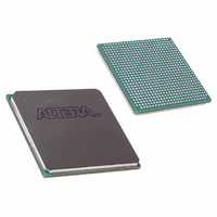
EP1SGX25DF672C5N Altera, EP1SGX25DF672C5N Datasheet - Page 232

EP1SGX25DF672C5N
Manufacturer Part Number
EP1SGX25DF672C5N
Description
IC STRATIX GX FPGA 25K 672-FBGA
Manufacturer
Altera
Series
Stratix® GXr
Datasheet
1.EP1SGX10CF672C7N.pdf
(272 pages)
Specifications of EP1SGX25DF672C5N
Number Of Logic Elements/cells
25660
Number Of Labs/clbs
2566
Total Ram Bits
1944576
Number Of I /o
455
Voltage - Supply
1.425 V ~ 1.575 V
Mounting Type
Surface Mount
Operating Temperature
0°C ~ 85°C
Package / Case
672-FBGA
Lead Free Status / RoHS Status
Lead free / RoHS Compliant
Number Of Gates
-
Available stocks
Company
Part Number
Manufacturer
Quantity
Price
Company:
Part Number:
EP1SGX25DF672C5N
Manufacturer:
ALTERA
Quantity:
3 000
- Current page: 232 of 272
- Download datasheet (3Mb)
Timing Model
Figure 6–4. Dual-Port RAM Timing Microparameter Waveform
6–30
Stratix GX Device Handbook, Volume 1
unreg_data-out
reg_data-out
wraddress
rdaddress
data-in
rdclock
wrclock
wren
rden
doutn-2
an-1
din-1
t
t
DATASU
WERESU
doutn-1
bn
t
DATAH
an
din
Figure 6–4
and M-RAM timing parameters shown in
t
t
R X _ F R E Q L O C K
R X _ F R E Q L O C K 2 P H A S E L O C K
Table 6–43. Stratix GX Reset & PLL Lock Time Parameter Descriptions
(Part 2 of 2)
t
doutn-1
WEREH
doutn
a0
b0
Symbol
shows the TriMatrix memory waveforms for the M512, M4K,
t
t
DATACO1
WEREH
t
DATACO2
a1
t
RC
doutn
dout0
The time until the clock recovery unit (CRU)
switches to data mode from lock to reference
mode.
The time until CRU phase locks to data after
switching from lock to data mode.
a2
b1
t
t
WADDRSU
a3
WERESU
dout0
Tables 6–39
Parameter
din4
a4
b2
through 6–41.
Altera Corporation
t
WADDRH
din5
a5
June 2006
b3
din6
a6
Related parts for EP1SGX25DF672C5N
Image
Part Number
Description
Manufacturer
Datasheet
Request
R

Part Number:
Description:
Stratix Gx Device Family Data Sheet
Manufacturer:
Altera Corporation
Datasheet:

Part Number:
Description:
CYCLONE II STARTER KIT EP2C20N
Manufacturer:
Altera
Datasheet:

Part Number:
Description:
CPLD, EP610 Family, ECMOS Process, 300 Gates, 16 Macro Cells, 16 Reg., 16 User I/Os, 5V Supply, 35 Speed Grade, 24DIP
Manufacturer:
Altera Corporation
Datasheet:

Part Number:
Description:
CPLD, EP610 Family, ECMOS Process, 300 Gates, 16 Macro Cells, 16 Reg., 16 User I/Os, 5V Supply, 15 Speed Grade, 24DIP
Manufacturer:
Altera Corporation
Datasheet:

Part Number:
Description:
Manufacturer:
Altera Corporation
Datasheet:

Part Number:
Description:
CPLD, EP610 Family, ECMOS Process, 300 Gates, 16 Macro Cells, 16 Reg., 16 User I/Os, 5V Supply, 30 Speed Grade, 24DIP
Manufacturer:
Altera Corporation
Datasheet:

Part Number:
Description:
High-performance, low-power erasable programmable logic devices with 8 macrocells, 10ns
Manufacturer:
Altera Corporation
Datasheet:

Part Number:
Description:
High-performance, low-power erasable programmable logic devices with 8 macrocells, 7ns
Manufacturer:
Altera Corporation
Datasheet:

Part Number:
Description:
Classic EPLD
Manufacturer:
Altera Corporation
Datasheet:

Part Number:
Description:
High-performance, low-power erasable programmable logic devices with 8 macrocells, 10ns
Manufacturer:
Altera Corporation
Datasheet:

Part Number:
Description:
Manufacturer:
Altera Corporation
Datasheet:

Part Number:
Description:
Manufacturer:
Altera Corporation
Datasheet:

Part Number:
Description:
Manufacturer:
Altera Corporation
Datasheet:


