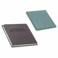
EP1SGX25CF672C7 Altera, EP1SGX25CF672C7 Datasheet - Page 105

EP1SGX25CF672C7
Manufacturer Part Number
EP1SGX25CF672C7
Description
IC STRATIX GX FPGA 25KLE 672FBGA
Manufacturer
Altera
Series
Stratix® GXr
Datasheet
1.EP1SGX10CF672C7N.pdf
(272 pages)
Specifications of EP1SGX25CF672C7
Number Of Logic Elements/cells
25660
Number Of Labs/clbs
2566
Total Ram Bits
1944576
Number Of I /o
455
Voltage - Supply
1.425 V ~ 1.575 V
Mounting Type
Surface Mount
Operating Temperature
0°C ~ 85°C
Package / Case
672-FBGA
Family Name
Stratix GX
Number Of Logic Blocks/elements
25660
# I/os (max)
455
Frequency (max)
4.38597GHz
Process Technology
SRAM
Operating Supply Voltage (typ)
1.5V
Logic Cells
25660
Ram Bits
1944576
Operating Supply Voltage (min)
1.425V
Operating Supply Voltage (max)
1.575V
Operating Temp Range
0C to 85C
Operating Temperature Classification
Commercial
Mounting
Surface Mount
Pin Count
672
Package Type
FC-FBGA
Lead Free Status / RoHS Status
Contains lead / RoHS non-compliant
Number Of Gates
-
Lead Free Status / Rohs Status
Not Compliant
Available stocks
Company
Part Number
Manufacturer
Quantity
Price
Part Number:
EP1SGX25CF672C7
Manufacturer:
ALTERA/阿尔特拉
Quantity:
20 000
- Current page: 105 of 272
- Download datasheet (3Mb)
Altera Corporation
February 2005
Table 4–11
column units (B1 to B6 and A1 to A6). It also shows the address and
control signal input connections to the row units (R1 to R11).
Unit Interface Block
Table 4–11. M-RAM Row & Column Interface Unit Signals
R10
R11
R1
R2
R3
R4
R5
R6
R7
R8
R9
B1
B2
B3
B4
B5
B6
A1
A2
A3
A4
A5
A6
shows the input and output data signal connections for the
byte_enable_a[7..0]
byte_enable_b[7..0]
datain_b[71..60]
datain_b[59..48]
datain_b[47..36]
datain_b[35..24]
datain_b[23..12]
datain_a[71..60]
datain_a[59..48]
datain_a[47..36]
datain_a[35..24]
datain_a[23..12]
addressa[15..8]
addressb[15..8]
datain_b[11..0]
datain_a[11..0]
addressa[7..0]
addressb[7..0]
Input SIgnals
clocken_a
clocken_b
renwe_a
clock_a
clock_b
renwe_b
-
-
-
-
Stratix GX Device Handbook, Volume 1
dataout_b[71..60]
dataout_b[59..48]
dataout_b[47..36]
dataout_b[35..24]
dataout_b[23..12]
dataout_a[71..60]
dataout_a[59..48]
dataout_a[47..36]
dataout_a[35..24]
dataout_a[23..12]
dataout_b[11..0]
dataout_a[11..0]
Stratix GX Architecture
Output Signals
4–39
Related parts for EP1SGX25CF672C7
Image
Part Number
Description
Manufacturer
Datasheet
Request
R

Part Number:
Description:
CYCLONE II STARTER KIT EP2C20N
Manufacturer:
Altera
Datasheet:

Part Number:
Description:
CPLD, EP610 Family, ECMOS Process, 300 Gates, 16 Macro Cells, 16 Reg., 16 User I/Os, 5V Supply, 35 Speed Grade, 24DIP
Manufacturer:
Altera Corporation
Datasheet:

Part Number:
Description:
CPLD, EP610 Family, ECMOS Process, 300 Gates, 16 Macro Cells, 16 Reg., 16 User I/Os, 5V Supply, 15 Speed Grade, 24DIP
Manufacturer:
Altera Corporation
Datasheet:

Part Number:
Description:
Manufacturer:
Altera Corporation
Datasheet:

Part Number:
Description:
CPLD, EP610 Family, ECMOS Process, 300 Gates, 16 Macro Cells, 16 Reg., 16 User I/Os, 5V Supply, 30 Speed Grade, 24DIP
Manufacturer:
Altera Corporation
Datasheet:

Part Number:
Description:
High-performance, low-power erasable programmable logic devices with 8 macrocells, 10ns
Manufacturer:
Altera Corporation
Datasheet:

Part Number:
Description:
High-performance, low-power erasable programmable logic devices with 8 macrocells, 7ns
Manufacturer:
Altera Corporation
Datasheet:

Part Number:
Description:
Classic EPLD
Manufacturer:
Altera Corporation
Datasheet:

Part Number:
Description:
High-performance, low-power erasable programmable logic devices with 8 macrocells, 10ns
Manufacturer:
Altera Corporation
Datasheet:

Part Number:
Description:
Manufacturer:
Altera Corporation
Datasheet:

Part Number:
Description:
Manufacturer:
Altera Corporation
Datasheet:

Part Number:
Description:
Manufacturer:
Altera Corporation
Datasheet:

Part Number:
Description:
CPLD, EP610 Family, ECMOS Process, 300 Gates, 16 Macro Cells, 16 Reg., 16 User I/Os, 5V Supply, 25 Speed Grade, 24DIP
Manufacturer:
Altera Corporation
Datasheet:


