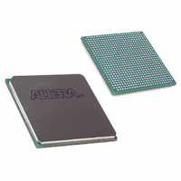
EP1SGX10DF672I6 Altera, EP1SGX10DF672I6 Datasheet - Page 6

EP1SGX10DF672I6
Manufacturer Part Number
EP1SGX10DF672I6
Description
IC STRATIX GX FPGA 10KLE 672FBGA
Manufacturer
Altera
Series
Stratix® GXr
Datasheet
1.EP1SGX10CF672C7N.pdf
(272 pages)
Specifications of EP1SGX10DF672I6
Number Of Logic Elements/cells
10570
Number Of Labs/clbs
1057
Total Ram Bits
920448
Number Of I /o
362
Voltage - Supply
1.425 V ~ 1.575 V
Mounting Type
Surface Mount
Operating Temperature
-40°C ~ 100°C
Package / Case
672-FBGA
Family Name
Stratix GX
Number Of Logic Blocks/elements
10570
# I/os (max)
362
Frequency (max)
5GHz
Process Technology
SRAM
Operating Supply Voltage (typ)
1.5V
Logic Cells
10570
Ram Bits
920448
Operating Supply Voltage (min)
1.425V
Operating Supply Voltage (max)
1.575V
Operating Temp Range
-40C to 100C
Operating Temperature Classification
Industrial
Mounting
Surface Mount
Pin Count
672
Package Type
FC-FBGA
Lead Free Status / RoHS Status
Contains lead / RoHS non-compliant
Number Of Gates
-
Lead Free Status / Rohs Status
Not Compliant
Available stocks
Company
Part Number
Manufacturer
Quantity
Price
- Current page: 6 of 272
- Download datasheet (3Mb)
High-Speed I/O Interface Functional Description
High-Speed I/O
Interface
Functional
Description
1–4
Stratix GX Device Handbook, Volume 1
The Stratix GX device family supports high-speed serial transceiver
blocks with CDR circuitry as well as source-synchronous interfaces. The
channels on the right side of the device use an embedded circuit
dedicated for receiving and transmitting high-speed serial data streams
to and from the system board. These channels are clustered in a
four-channel serial transceiver building block and deliver high-speed
bidirectional point-to-point data transmissions to provide up to
3.1875 Gbps of full-duplex data transmission per channel. The channels
on the left side of the device support source-synchronous data transfers
at up to 1 Gbps using LVDS, LVPECL, 3.3-V PCML, or HyperTransport
technology I/O standards.
The differential source-synchronous serial interface and the high-speed
serial interface are described in the Stratix GX Transceivers chapter of the
Stratix GX Device Handbook, Volume 1.
Note to
(1)
EP1SGX25D
EP1SGX25F
EP1SGX40D
EP1SGX40G
Pitch (mm)
Area (mm
Length
EP1SGX10
EP1SGX25
EP1SGX40
Table 1–2. Stratix GX Package Options & I/O Pin Counts (Part 2
of 2)
Table 1–3. Stratix GX FineLine BGA Package Sizes
Table 1–4. Stratix GX Device Speed Grades
The number of I/O pins listed for each package includes dedicated clock pins and
dedicated fast I/O pins. However, these numbers do not include high-speed or
clock reference pins for high-speed I/O standards.
Device
×
Table
Device
width (mm
2
Note (1)
Dimension
)
1–2:
×
mm)
672-Pin FineLine BGA
672-Pin FineLine BGA
Figure 1–1
-5, -6, -7
-5, -6, -7
455
672 Pin
27
1.00
shows the Stratix GX I/O blocks.
729
×
27
1,020-pin FineLine BGA
1,020-Pin FineLine BGA
Altera Corporation
-5, -6, -7
-5, -6, -7
1,020 Pin
33
607
607
624
624
February 2005
1,089
1.00
×
33
Related parts for EP1SGX10DF672I6
Image
Part Number
Description
Manufacturer
Datasheet
Request
R

Part Number:
Description:
CYCLONE II STARTER KIT EP2C20N
Manufacturer:
Altera
Datasheet:

Part Number:
Description:
CPLD, EP610 Family, ECMOS Process, 300 Gates, 16 Macro Cells, 16 Reg., 16 User I/Os, 5V Supply, 35 Speed Grade, 24DIP
Manufacturer:
Altera Corporation
Datasheet:

Part Number:
Description:
CPLD, EP610 Family, ECMOS Process, 300 Gates, 16 Macro Cells, 16 Reg., 16 User I/Os, 5V Supply, 15 Speed Grade, 24DIP
Manufacturer:
Altera Corporation
Datasheet:

Part Number:
Description:
Manufacturer:
Altera Corporation
Datasheet:

Part Number:
Description:
CPLD, EP610 Family, ECMOS Process, 300 Gates, 16 Macro Cells, 16 Reg., 16 User I/Os, 5V Supply, 30 Speed Grade, 24DIP
Manufacturer:
Altera Corporation
Datasheet:

Part Number:
Description:
High-performance, low-power erasable programmable logic devices with 8 macrocells, 10ns
Manufacturer:
Altera Corporation
Datasheet:

Part Number:
Description:
High-performance, low-power erasable programmable logic devices with 8 macrocells, 7ns
Manufacturer:
Altera Corporation
Datasheet:

Part Number:
Description:
Classic EPLD
Manufacturer:
Altera Corporation
Datasheet:

Part Number:
Description:
High-performance, low-power erasable programmable logic devices with 8 macrocells, 10ns
Manufacturer:
Altera Corporation
Datasheet:

Part Number:
Description:
Manufacturer:
Altera Corporation
Datasheet:

Part Number:
Description:
Manufacturer:
Altera Corporation
Datasheet:

Part Number:
Description:
Manufacturer:
Altera Corporation
Datasheet:

Part Number:
Description:
CPLD, EP610 Family, ECMOS Process, 300 Gates, 16 Macro Cells, 16 Reg., 16 User I/Os, 5V Supply, 25 Speed Grade, 24DIP
Manufacturer:
Altera Corporation
Datasheet:


