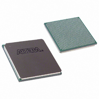
EP3C120F780I7 Altera, EP3C120F780I7 Datasheet - Page 155

EP3C120F780I7
Manufacturer Part Number
EP3C120F780I7
Description
IC CYCLONE III FPGA 120K 780FBGA
Manufacturer
Altera
Series
Cyclone® IIIr
Datasheets
1.EP3C5F256C8N.pdf
(5 pages)
2.EP3C5F256C8N.pdf
(34 pages)
3.EP3C5F256C8N.pdf
(66 pages)
4.EP3C5F256C8N.pdf
(14 pages)
5.EP3C5F256C8N.pdf
(76 pages)
6.EP3C120F780I7.pdf
(274 pages)
Specifications of EP3C120F780I7
Number Of Logic Elements/cells
119088
Number Of Labs/clbs
7443
Total Ram Bits
3981312
Number Of I /o
531
Voltage - Supply
1.15 V ~ 1.25 V
Mounting Type
Surface Mount
Operating Temperature
-40°C ~ 100°C
Package / Case
780-FBGA
Family Name
Cyclone III
Number Of Logic Blocks/elements
119088
# I/os (max)
531
Frequency (max)
437.5MHz
Process Technology
65nm
Operating Supply Voltage (typ)
1.2V
Logic Cells
119088
Ram Bits
3981312
Operating Supply Voltage (min)
1.15V
Operating Supply Voltage (max)
1.25V
Operating Temp Range
-40C to 100C
Operating Temperature Classification
Industrial
Mounting
Surface Mount
Pin Count
780
Package Type
FBGA
For Use With
544-2589 - KIT DEV EMB CYCLONE III EDITION544-2566 - KIT DEV DSP CYCLONE III EDITION544-2444 - KIT DEV CYCLONE III EP3C120
Lead Free Status / RoHS Status
Contains lead / RoHS non-compliant
Number Of Gates
-
Lead Free Status / Rohs Status
Not Compliant
Available stocks
Company
Part Number
Manufacturer
Quantity
Price
Part Number:
EP3C120F780I7
Manufacturer:
ALTERA/阿尔特拉
Quantity:
20 000
Company:
Part Number:
EP3C120F780I7N
Manufacturer:
ALTERA
Quantity:
118
Chapter 8: External Memory Interfaces in the Cyclone III Device Family
Cyclone III Device Family Memory Interfaces Features
Figure 8–4. Cyclone III Device Family DDR Input Registers
© January 2010 Altera Corporation
dataout_h
dataout_l
Figure 8–4
The DDR data is first fed to two registers, input register A
■
■
■
The data from the DDR input register is fed to two registers, sync_reg_h and
sync_reg_l, then the data is typically transferred to a FIFO block to synchronize the
two data streams to the rising edge of the system clock. Because the read-capture
clock is generated by the PLL, the read-data strobe signal (DQS or CQ) is not used
during read operation in Cyclone III device family; hence, postamble is not a concern
in this case.
Input register A
Input register B
Register C
shows Cyclone III device family DDR input registers.
I
aligns the data before it is synchronized with the system clock
I
I
captures the DDR data present during the falling edge of the clock
captures the DDR data present during the rising edge of the clock
DDR Input Registers in Cyclone III Device Family
Register C
Register
LE
I
Input Register A
Input Register B
neg_reg_out
Register
Register
LE
LE
I
I
Capture Clock
Cyclone III Device Handbook, Volume 1
I
and input register B
PLL
DQ
I
.
8–11


