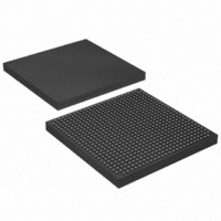
EP1S25F672C8 Altera, EP1S25F672C8 Datasheet - Page 108

EP1S25F672C8
Manufacturer Part Number
EP1S25F672C8
Description
IC STRATIX FPGA 25K LE 672-FBGA
Manufacturer
Altera
Series
Stratix®r
Datasheet
1.EP1S10F780C7.pdf
(276 pages)
Specifications of EP1S25F672C8
Number Of Logic Elements/cells
25660
Number Of Labs/clbs
2566
Total Ram Bits
1944576
Number Of I /o
473
Voltage - Supply
1.425 V ~ 1.575 V
Mounting Type
Surface Mount
Operating Temperature
0°C ~ 85°C
Package / Case
672-FBGA
Lead Free Status / RoHS Status
Contains lead / RoHS non-compliant
Number Of Gates
-
Other names
544-1119
Available stocks
Company
Part Number
Manufacturer
Quantity
Price
Company:
Part Number:
EP1S25F672C8
Manufacturer:
AD
Quantity:
2 562
Company:
Part Number:
EP1S25F672C8
Manufacturer:
ALTERA
Quantity:
3 000
Part Number:
EP1S25F672C8
Manufacturer:
ALTERA
Quantity:
20 000
Company:
Part Number:
EP1S25F672C8N
Manufacturer:
ALTERA
Quantity:
465
Part Number:
EP1S25F672C8N
Manufacturer:
ALTERA/阿尔特拉
Quantity:
20 000
- Current page: 108 of 276
- Download datasheet (4Mb)
PLLs & Clock Networks
2–94
Stratix Device Handbook, Volume 1
Any of the four external output counters can drive the single-ended or
differential clock outputs for PLLs 5 and 6. This means one counter or
frequency can drive all output pins available from PLL 5 or PLL 6. Each
pair of output pins (four pins total) has dedicated VCC and GND pins to
reduce the output clock’s overall jitter by providing improved isolation
from switching I/O pins.
For PLLs 5 and 6, each pin of a single-ended output pair can either be in
phase or 180° out of phase. The clock output pin pairs support the same
I/O standards as standard output pins (in the top and bottom banks) as
well as LVDS, LVPECL, 3.3-V PCML, HyperTransport technology,
differential HSTL, and differential SSTL.
standards the enhanced PLL clock pins support. When in single-ended or
differential mode, the two outputs operate off the same power supply.
Both outputs use the same standards in single-ended mode to maintain
performance. You can also use the external clock output pins as user
output pins if external enhanced PLL clocking is not needed.
LVTTL
LVCMOS
2.5 V
1.8 V
1.5 V
3.3-V PCI
3.3-V PCI-X 1.0
LVPECL
3.3-V PCML
LVDS
HyperTransport technology
Differential HSTL
Differential SSTL
3.3-V GTL
3.3-V GTL+
1.5-V HSTL Class I
Table 2–20. I/O Standards Supported for Enhanced PLL Pins (Part 1 of 2)
I/O Standard
INCLK
v
v
v
v
v
v
v
v
v
v
v
v
v
v
v
FBIN
v
v
v
v
v
v
v
v
v
v
v
v
v
v
Table 2–20
Input
PLLENABLE
shows which I/O
v
v
Altera Corporation
EXTCLK
July 2005
Output
v
v
v
v
v
v
v
v
v
v
v
v
v
v
v
v
Related parts for EP1S25F672C8
Image
Part Number
Description
Manufacturer
Datasheet
Request
R

Part Number:
Description:
CYCLONE II STARTER KIT EP2C20N
Manufacturer:
Altera
Datasheet:

Part Number:
Description:
CPLD, EP610 Family, ECMOS Process, 300 Gates, 16 Macro Cells, 16 Reg., 16 User I/Os, 5V Supply, 35 Speed Grade, 24DIP
Manufacturer:
Altera Corporation
Datasheet:

Part Number:
Description:
CPLD, EP610 Family, ECMOS Process, 300 Gates, 16 Macro Cells, 16 Reg., 16 User I/Os, 5V Supply, 15 Speed Grade, 24DIP
Manufacturer:
Altera Corporation
Datasheet:

Part Number:
Description:
Manufacturer:
Altera Corporation
Datasheet:

Part Number:
Description:
CPLD, EP610 Family, ECMOS Process, 300 Gates, 16 Macro Cells, 16 Reg., 16 User I/Os, 5V Supply, 30 Speed Grade, 24DIP
Manufacturer:
Altera Corporation
Datasheet:

Part Number:
Description:
High-performance, low-power erasable programmable logic devices with 8 macrocells, 10ns
Manufacturer:
Altera Corporation
Datasheet:

Part Number:
Description:
High-performance, low-power erasable programmable logic devices with 8 macrocells, 7ns
Manufacturer:
Altera Corporation
Datasheet:

Part Number:
Description:
Classic EPLD
Manufacturer:
Altera Corporation
Datasheet:

Part Number:
Description:
High-performance, low-power erasable programmable logic devices with 8 macrocells, 10ns
Manufacturer:
Altera Corporation
Datasheet:

Part Number:
Description:
Manufacturer:
Altera Corporation
Datasheet:

Part Number:
Description:
Manufacturer:
Altera Corporation
Datasheet:

Part Number:
Description:
Manufacturer:
Altera Corporation
Datasheet:

Part Number:
Description:
CPLD, EP610 Family, ECMOS Process, 300 Gates, 16 Macro Cells, 16 Reg., 16 User I/Os, 5V Supply, 25 Speed Grade, 24DIP
Manufacturer:
Altera Corporation
Datasheet:


