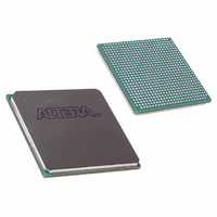
EP2S30F672C5 Altera, EP2S30F672C5 Datasheet - Page 145

EP2S30F672C5
Manufacturer Part Number
EP2S30F672C5
Description
IC STRATIX II FPGA 30K 672-FBGA
Manufacturer
Altera
Series
Stratix® IIr
Datasheet
1.EP2S15F484I4N.pdf
(238 pages)
Specifications of EP2S30F672C5
Number Of Logic Elements/cells
33880
Number Of Labs/clbs
1694
Total Ram Bits
1369728
Number Of I /o
500
Voltage - Supply
1.15 V ~ 1.25 V
Mounting Type
Surface Mount
Operating Temperature
0°C ~ 85°C
Package / Case
672-FBGA
Family Name
Stratix II
Number Of Logic Blocks/elements
33880
# I/os (max)
500
Frequency (max)
609.76MHz
Process Technology
90nm (CMOS)
Operating Supply Voltage (typ)
1.2V
Logic Cells
33880
Ram Bits
1369728
Operating Supply Voltage (min)
1.15V
Operating Supply Voltage (max)
1.25V
Operating Temp Range
0C to 85C
Operating Temperature Classification
Commercial
Mounting
Surface Mount
Pin Count
672
Package Type
FBGA
Lead Free Status / RoHS Status
Contains lead / RoHS non-compliant
Number Of Gates
-
Lead Free Status / Rohs Status
Not Compliant
Other names
544-1126
Available stocks
Company
Part Number
Manufacturer
Quantity
Price
Company:
Part Number:
EP2S30F672C5K
Manufacturer:
ALTERA
Quantity:
220
Company:
Part Number:
EP2S30F672C5N
Manufacturer:
ALTERA
Quantity:
238
Part Number:
EP2S30F672C5N
Manufacturer:
ALTERA/阿尔特拉
Quantity:
20 000
Altera Corporation
April 2011
Note to
(1)
V
V
V
V
V
R
V
V
V
V
Δ V
V
Δ V
R
V
V
Table 5–12. LVPECL Specifications
Table 5–13. HyperTransport Technology Specifications
Table 5–14. 3.3-V PCI Specifications (Part 1 of 2)
Symbol
Symbol
Symbol
CCIO
ID
ICM
OD
OCM
CCIO
ID
ICM
OD
OCM
CCIO
IH
L
L
OD
OCM
The top and bottom clock input differential buffers in I/O banks 3, 4, 7, and 8 are powered by V
The PLL clock output/feedback differential buffers are powered by VCC_PLL_OUT. For differential clock
output/feedback operation, VCC_PLL_OUT should be connected to 3.3 V.
(1)
Table
I/O supply voltage
Input differential voltage
swing (single-ended)
Input common mode voltage
Output differential voltage
(single-ended)
Output common mode
voltage
Receiver differential input
resistor
I/O supply voltage for left and
right I/O banks (1, 2, 5, and 6)
Input differential voltage swing
(single-ended)
Input common mode voltage
Output differential voltage
(single-ended)
Change in V
and low
Output common mode voltage R
Change in V
and low
Receiver differential input
resistor
Output supply voltage
High-level input voltage
5–12:
Parameter
Parameter
Parameter
OCM
OD
between high
between high
R
R
L
L
R
R
R
R
R
= 100 Ω
= 100 Ω
Conditions
L
L
L
L
L
L
Conditions
Conditions
= 100 Ω
= 100 Ω
= 100 Ω
= 100 Ω
= 100 Ω
= 100 Ω
0.5 × V
Minimum
Minimum
Minimum
3.135
1,650
2.375
300
525
300
385
400
440
1.0
3.0
90
90
CCIO
Stratix II Device Handbook, Volume 1
DC & Switching Characteristics
Typical
Typical
Typical
3.300
2.500
600
100
600
600
600
600
100
3.3
V
Maximum
Maximum
Maximum
CCIO
CCINT
3.465
1,000
2,250
2.625
970
110
900
845
820
780
110
2.5
3.6
75
50
+ 0.5
, not V
CCIO
Unit
Unit
Unit
mV
mV
mV
mV
mV
mV
mV
mV
mV
5–9
V
V
Ω
Ω
V
V
V
.


