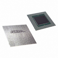
EP20K400EBC652-3N Altera, EP20K400EBC652-3N Datasheet - Page 39

EP20K400EBC652-3N
Manufacturer Part Number
EP20K400EBC652-3N
Description
IC APEX 20KE FPGA 400K 652-BGA
Manufacturer
Altera
Series
APEX-20K®r
Datasheet
1.EP20K30ETC144-3.pdf
(117 pages)
Specifications of EP20K400EBC652-3N
Number Of Logic Elements/cells
16640
Number Of Labs/clbs
1664
Total Ram Bits
212992
Number Of I /o
488
Number Of Gates
1052000
Voltage - Supply
1.71 V ~ 1.89 V
Mounting Type
Surface Mount
Operating Temperature
0°C ~ 85°C
Package / Case
652-BGA
Family Name
APEX 20K
Number Of Usable Gates
400000
Number Of Logic Blocks/elements
16640
# I/os (max)
488
Frequency (max)
213MHz
Process Technology
SRAM
Operating Supply Voltage (typ)
1.8V
Logic Cells
16640
Ram Bits
212992
Device System Gates
1052000
Operating Supply Voltage (min)
1.71V
Operating Supply Voltage (max)
1.89V
Operating Temp Range
0C to 85C
Operating Temperature Classification
Commercial
Mounting
Surface Mount
Pin Count
652
Package Type
BGA
Lead Free Status / RoHS Status
Lead free / RoHS Compliant
Available stocks
Company
Part Number
Manufacturer
Quantity
Price
Altera Corporation
Figure 25. APEX 20K Bidirectional I/O Registers
Note to
(1)
or Local Interconnect
The output enable and input registers are LE registers in the LAB adjacent to the bidirectional pin.
Row, Column,
Figure
25:
4 Dedicated
Inputs
Clock Inputs
2 Dedicated
2
Peripheral Control
Bus
12
OE[7..0]
VCC
CLK[1..0]
CLK[3..2]
ENA[5..0]
CLRn[1..0]
VCC
Input Pin to Input
Core to Output
Register Delay
VCC
VCC
Register Delay
VCC
VCC
VCC
APEX 20K Programmable Logic Device Family Data Sheet
Chip-Wide
Chip-Wide
Chip-Wide Reset
Input Pin to
Reset
Reset
Core Delay
Note (1)
Output Enable
Output Register
Chip-Wide
Input Register
OE Register
D
ENA
D
ENA
D
ENA
CLRN
CLRN
CLRN
Q
Q
Q
Open-Drain
Slew-Rate
Output
Control
Output Register
t
CO
Delay
VCCIO
Optional
PCI Clamp
39


