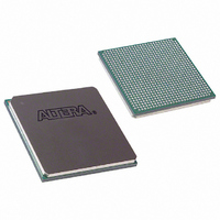
EP3C40F780I7 Altera, EP3C40F780I7 Datasheet - Page 70

EP3C40F780I7
Manufacturer Part Number
EP3C40F780I7
Description
IC CYCLONE III FPGA 40K 780 FBGA
Manufacturer
Altera
Series
Cyclone® IIIr
Datasheets
1.EP3C5F256C8N.pdf
(5 pages)
2.EP3C5F256C8N.pdf
(34 pages)
3.EP3C5F256C8N.pdf
(66 pages)
4.EP3C5F256C8N.pdf
(14 pages)
5.EP3C5F256C8N.pdf
(76 pages)
6.EP3C40F780I7.pdf
(274 pages)
Specifications of EP3C40F780I7
Number Of Logic Elements/cells
39600
Number Of Labs/clbs
2475
Total Ram Bits
1161216
Number Of I /o
535
Voltage - Supply
1.15 V ~ 1.25 V
Mounting Type
Surface Mount
Operating Temperature
-40°C ~ 100°C
Package / Case
780-FBGA
Family Name
Cyclone III
Number Of Logic Blocks/elements
39600
# I/os (max)
535
Frequency (max)
437.5MHz
Process Technology
65nm
Operating Supply Voltage (typ)
1.2V
Logic Cells
39600
Ram Bits
1161216
Operating Supply Voltage (min)
1.15V
Operating Supply Voltage (max)
1.25V
Operating Temp Range
-40C to 100C
Operating Temperature Classification
Industrial
Mounting
Surface Mount
Pin Count
780
Package Type
FBGA
Lead Free Status / RoHS Status
Contains lead / RoHS non-compliant
Number Of Gates
-
Lead Free Status / Rohs Status
Not Compliant
Available stocks
Company
Part Number
Manufacturer
Quantity
Price
Company:
Part Number:
EP3C40F780I7N
Manufacturer:
MINGTEK
Quantity:
2 300
Company:
Part Number:
EP3C40F780I7N
Manufacturer:
ALTERA20
Quantity:
576
Part Number:
EP3C40F780I7N
Manufacturer:
ALTERA/阿尔特拉
Quantity:
20 000
2–26
Glossary
Table 2–39. Glossary (Part 1 of 5)
Cyclone III Device Handbook, Volume 2
Letter
M
D
G
H
N
O
A
B
C
E
F
K
L
I
J
f
GCLK
GCLK PLL
HSIODR
Input Waveforms
for the SSTL
Differential I/O
Standard
JTAG Waveform
HS CLK
Term
—
—
—
—
—
—
—
—
—
—
Table 2–39
V
Captured
High-speed I/O Block: High-speed receiver and transmitter input and output clock frequency.
Input pin directly to the global clock network.
High-speed I/O Block: Maximum and minimum LVDS data transfer rate (HSIODR = 1/TUI).
Input pin to the global clock network through the PLL.
SWING
Driven
Signal
Signal
to be
to be
TMS
TDO
TCK
TDI
lists the glossary for this chapter.
t
JCH
t
t
JSZX
JPZX
t
JCP
t
JSSU
t
JCL
t
JSH
t
t
JPCO
JSCO
t
t
JPSU_TDI
JPSU_TMS
Definitions
—
—
—
—
—
—
—
—
—
—
t
Chapter 2: Cyclone III LS Device Data Sheet
t
JSXZ
JPH
© December 2009 Altera Corporation
t
JPXZ
V
V
V
REF
IH
IL
Glossary


