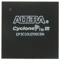
EP3C10U256C6N Altera, EP3C10U256C6N Datasheet - Page 18

EP3C10U256C6N
Manufacturer Part Number
EP3C10U256C6N
Description
IC CYCLONE III FPGA 10K 256-UBGA
Manufacturer
Altera
Series
Cyclone® IIIr
Datasheets
1.EP3C5F256C8N.pdf
(5 pages)
2.EP3C5F256C8N.pdf
(34 pages)
3.EP3C5F256C8N.pdf
(66 pages)
4.EP3C5F256C8N.pdf
(14 pages)
5.EP3C5F256C8N.pdf
(76 pages)
6.EP3C10U256C6N.pdf
(274 pages)
Specifications of EP3C10U256C6N
Number Of Logic Elements/cells
10320
Number Of Labs/clbs
645
Total Ram Bits
423936
Number Of I /o
182
Voltage - Supply
1.15 V ~ 1.25 V
Mounting Type
Surface Mount
Operating Temperature
0°C ~ 85°C
Package / Case
256-UBGA
Family Name
Cyclone III
Number Of Logic Blocks/elements
10320
# I/os (max)
182
Frequency (max)
500MHz
Process Technology
65nm
Operating Supply Voltage (typ)
1.2V
Logic Cells
10320
Ram Bits
423936
Operating Supply Voltage (min)
1.15V
Operating Supply Voltage (max)
1.25V
Operating Temp Range
0C to 85C
Operating Temperature Classification
Commercial
Mounting
Surface Mount
Pin Count
256
Package Type
UFBGA
For Use With
544-2601 - KIT DEV CYCLONE III LS EP3CLS200544-2411 - KIT DEV NIOS II CYCLONE III ED.
Lead Free Status / RoHS Status
Lead free / RoHS Compliant
Number Of Gates
-
Lead Free Status / Rohs Status
Compliant
Other names
544-2433
EP3C10U256C6N
EP3C10U256C6N
Available stocks
Company
Part Number
Manufacturer
Quantity
Price
1–8
Cyclone III Device Handbook, Volume 2
Table 1–7
Table 1–7. Cyclone III Devices Series OCT with Calibration at Device Power-Up Specifications
The OCT resistance may vary with the variation of temperature and voltage after
calibration at device power-up. Use
OCT resistance considering the variations after calibration at device power-up.
Table 1–8
temperature.
Table 1–8. Cyclone III Devices OCT Variation After Calibration at Device Power-Up
Equation 1–1.
ΔR
ΔR
For ΔR
For ΔR
MF = MF
R
Notes to
(1) T
(2) T
(3) MF is multiplication factor.
(4) R
(5) R
(6) Subscript × refers to both
(7) ΔR
(8) ΔR
(9) dR/dT is the change percentage of resistance with temperature after calibration at device power-up.
(10) dR/dV is the change percentage of resistance with voltage after calibration at device power-up.
(11) V
(12) V
Series OCT with
calibration at device
power-up
final
V
T
= (T
= R
= (V
2
1
2
1
final
initial
is the final temperature.
is the initial temperature.
is final voltage.
is the initial voltage.
T
x
x
V
Description
initia l
Equation
is variation of resistance with temperature.
Nominal Voltage
< 0; MF
> 0; MF
is variation of resistance with voltage.
2
2
is final resistance.
V
is initial resistance.
– T
– V
× MF
× MF –––––
lists the OCT calibration accuracy at device power-up.
lists the change percentage of the OCT resistance with voltage and
1
1
) × dR/dT –––––
) × 1000 × dR/dV –––––
T
3.0
2.5
1.8
1.5
1.2
x
x
–––––
= 1/ (|ΔR
1–1:
(Note
= ΔR
x
/100 + 1 –––––
1), (2), (3), (4), (5),
(11)
(12)
x
|/100 + 1) –––––
V
and
V
(8)
CCIO
T
3.0
2.5
1.8
1.5
1.2
.
(V)
(10)
(7)
Commercial Max
Table 1–8
(6)
(9)
dR/dT (%/°C)
0.262
0.234
0.219
0.199
0.161
±10
±10
±10
±10
±10
and
Calibration Accuracy
Equation 1–1
Industrial and Automotive
Chapter 1: Cyclone III Device Data Sheet
© January 2010 Altera Corporation
Max
±10
±10
±10
±10
±10
to determine the final
dR/dV (%/mV)
Electrical Characteristics
–0.026
–0.039
–0.086
–0.136
–0.288
Unit
%
%
%
%
%


