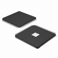
EP3C5E144I7 Altera, EP3C5E144I7 Datasheet - Page 74

EP3C5E144I7
Manufacturer Part Number
EP3C5E144I7
Description
IC CYCLONE III FPGA 5K 144 EQFP
Manufacturer
Altera
Series
Cyclone® IIIr
Datasheets
1.EP3C5F256C8N.pdf
(5 pages)
2.EP3C5F256C8N.pdf
(34 pages)
3.EP3C5F256C8N.pdf
(66 pages)
4.EP3C5F256C8N.pdf
(14 pages)
5.EP3C5F256C8N.pdf
(76 pages)
Specifications of EP3C5E144I7
Number Of Logic Elements/cells
5136
Number Of Labs/clbs
321
Total Ram Bits
423936
Number Of I /o
94
Voltage - Supply
1.15 V ~ 1.25 V
Mounting Type
Surface Mount
Operating Temperature
-40°C ~ 100°C
Package / Case
144-EQFP
Lead Free Status / RoHS Status
Contains lead / RoHS non-compliant
Number Of Gates
-
Available stocks
Company
Part Number
Manufacturer
Quantity
Price
Company:
Part Number:
EP3C5E144I7N
Manufacturer:
Altera
Quantity:
135
Company:
Part Number:
EP3C5E144I7N
Manufacturer:
ALTERA32
Quantity:
345
Part Number:
EP3C5E144I7N
Manufacturer:
ALTERA/阿尔特拉
Quantity:
20 000
2–30
Table 2–39. Glossary (Part 5 of 5)
Cyclone III Device Handbook, Volume 2
Letter
W
V
X
Y
Z
V
V
V
V
V
V
V
V
V
V
V
V
V
V
V
V
V
V
V
V
V
V
V
V
V
C M( DC)
DIF( AC )
DIF( DC)
IC M
ID
IH
IH(A C)
IH(DC )
IL
IL ( AC )
IL ( DC)
IN
OC M
OD
OH
OL
OS
OX ( AC)
REF
REF (A C)
REF (DC )
S WING (A C)
S WING (DC )
TT
X ( AC)
Term
—
—
—
—
DC common mode input voltage.
AC differential Input Voltage—The minimum AC input differential voltage required for
switching.
DC differential Input Voltage—The minimum DC input differential voltage required for
switching.
Input Common Mode Voltage—The common mode of the differential signal at the receiver.
Input differential Voltage Swing—The difference in voltage between the positive and
complementary conductors of a differential transmission at the receiver.
Voltage Input High—The minimum positive voltage applied to the input that is accepted by
the device as a logic high.
High-level AC input voltage.
High-level DC input voltage.
Voltage Input Low—The maximum positive voltage applied to the input that is accepted by
the device as a logic low.
Low-level AC input voltage.
Low-level DC input voltage.
DC input voltage.
Output Common Mode Voltage—The common mode of the differential signal at the
transmitter.
Output differential Voltage Swing—The difference in voltage between the positive and
complementary conductors of a differential transmission at the transmitter. V
Voltage Output High—The maximum positive voltage from an output that the device
considers will be accepted as the minimum positive high level.
Voltage Output Low—The maximum positive voltage from an output that the device considers
will be accepted as the maximum positive low level.
Output offset voltage—V
AC differential Output cross point voltage—The voltage at which the differential output signals
must cross.
Reference voltage for the SSTL and HSTL I/O standards.
AC input reference voltage for the SSTL and HSTL I/O standards. V
peak-to-peak AC noise on V
DC input reference voltage for the SSTL and HSTL I/O standards.
AC differential Input Voltage—AC Input differential voltage required for switching. Refer to
Input Waveforms for the SSTL Differential I/O Standard.
DC differential Input Voltage—DC Input differential voltage required for switching. Refer to
Input Waveforms for the SSTL Differential I/O Standard.
Termination voltage for the SSTL and HSTL I/O standards.
AC differential Input cross point Voltage—The voltage at which the differential input signals
must cross.
OS
= (V
REF
must not exceed 2% of V
OH
+ V
OL
) / 2.
Definitions
—
—
—
—
REF (DC)
Chapter 2: Cyclone III LS Device Data Sheet
.
© December 2009 Altera Corporation
REF (AC )
= V
REF (DC)
OD
= V
+ noise. The
OH
– V
Glossary
OL
.


