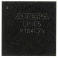
EP3C5M164C7N Altera, EP3C5M164C7N Datasheet - Page 48

EP3C5M164C7N
Manufacturer Part Number
EP3C5M164C7N
Description
IC CYCLONE III FPGA 5K 164 MBGA
Manufacturer
Altera
Series
Cyclone® IIIr
Datasheets
1.EP3C5F256C8N.pdf
(5 pages)
2.EP3C5F256C8N.pdf
(34 pages)
3.EP3C5F256C8N.pdf
(66 pages)
4.EP3C5F256C8N.pdf
(14 pages)
5.EP3C5F256C8N.pdf
(76 pages)
6.EP3C5M164C7N.pdf
(274 pages)
Specifications of EP3C5M164C7N
Number Of Logic Elements/cells
5136
Number Of Labs/clbs
321
Total Ram Bits
423936
Number Of I /o
106
Voltage - Supply
1.15 V ~ 1.25 V
Mounting Type
Surface Mount
Operating Temperature
0°C ~ 85°C
Package / Case
164-MBGA
Family Name
Cyclone III
Number Of Logic Blocks/elements
5136
# I/os (max)
106
Frequency (max)
437.5MHz
Process Technology
65nm
Operating Supply Voltage (typ)
1.2V
Logic Cells
5136
Ram Bits
423936
Operating Supply Voltage (min)
1.15V
Operating Supply Voltage (max)
1.25V
Operating Temp Range
0C to 85C
Operating Temperature Classification
Commercial
Mounting
Surface Mount
Pin Count
164
Package Type
MBGA
For Use With
544-2601 - KIT DEV CYCLONE III LS EP3CLS200544-2411 - KIT DEV NIOS II CYCLONE III ED.
Lead Free Status / RoHS Status
Lead free / RoHS Compliant
Number Of Gates
-
Lead Free Status / Rohs Status
Compliant
Other names
544-2559
Available stocks
Company
Part Number
Manufacturer
Quantity
Price
Company:
Part Number:
EP3C5M164C7N
Manufacturer:
ALTERA
Quantity:
526
2–4
Table 2–3. Cyclone III LS Devices Recommended Operating Conditions
Cyclone III Device Handbook, Volume 2
V
V
V
T
t
I
Notes to
(1) V
(2) V
(3) V
(4) Power-on reset (POR) time for Standard POR ranges from 50 to 200 ms. Each individual power supply must reach the recommended operating
(5) POR time for Fast POR ranges from 3 to 9 ms. Each individual power supply must reach the recommended operating range within 3 ms.
(6) All input buffers are powered by the V
RAM P
Diode
J
C CB AT
I
O
Symbol
locked-loops [PLLs}), and must be powered up and powered down at the same time.
range within 50 ms.
CC IO
CC D_P LL
CC
must rise monotonically.
Table
for all I/O banks must be powered up during device operation. All V
must always be connected to V
2–3:
Battery back-up power supply for design
security volatile key register
Input voltage
Output voltage
Operating junction temperature
Power supply ramptime
Magnitude of DC current across
PCI-clamp diode when enabled
DC Characteristics
This section lists the I/O leakage current, pin capacitance, on-chip termination (OCT)
tolerance, and bus hold specifications for Cyclone III LS devices.
Supply Current
Supply current is the current the device draws after the device is configured with no
inputs or outputs toggling and no activity in the device. Use the Excel-based Early
Power Estimator (EPE) to get the supply current estimates for your design because
these currents vary largely with the resources you use.
Table 2–4
Table 2–4. Cyclone III LS Devices I/O Pin Leakage Current
Symbol
I
I
Notes to
(1) This value is specified for normal device operation. The value varies during device power-up. This applies for all
(2) The 10 μA I/O leakage current limit is applicable when the internal clamping diode is off. A higher current can be
I
OZ
V
observed when the diode is on.
CC IO
Parameter
Table
settings (3.3, 3.0, 2.5, 1.8, 1.5, and 1.2 V).
Input Pin Leakage Current V
Tri-stated I/O Pin Leakage
Current
lists the I/O pin leakage current for Cyclone III LS devices.
C CIO
CCINT
2–4:
supply.
through a decoupling capacitor and ferrite bead.
Parameter
V
For commercial use
I
O
Standard POR
For industrial use
= V
= V
CCA
Fast POR
Conditions
Conditions
pins must be powered to 2.5 V (even when you do not use phase
CC IOM AX
CC IOMA X
—
—
—
—
(Note 1)
to 0 V
to 0 V
(5)
(4)
,
(2)
(Note 1)
Chapter 2: Cyclone III LS Device Data Sheet
(Part 2 of 2)
Min
–10
–10
50 µs
50 µs
–0.5
Min
–40
1.2
—
© December 2009 Altera Corporation
0
0
,
(2)
Typ
—
—
Typ
3.0
—
—
—
—
—
—
—
Electrical Characteristics
50 ms
Max
3 ms
Max
10
10
V
100
3.3
3.6
85
10
C CIO
Unit
Unit
mA
μA
μA
°C
°C
—
—
V
V
V


