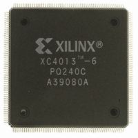
XC4013-6PQ240C Xilinx Inc, XC4013-6PQ240C Datasheet - Page 9

XC4013-6PQ240C
Manufacturer Part Number
XC4013-6PQ240C
Description
IC LOGIC CL ARRAY 13K GAT 240PQ
Manufacturer
Xilinx Inc
Series
XC4000r
Datasheet
1.XC4003-6PQ100C.pdf
(40 pages)
Specifications of XC4013-6PQ240C
Number Of Logic Elements/cells
1368
Number Of Labs/clbs
576
Total Ram Bits
18432
Number Of I /o
192
Number Of Gates
13000
Voltage - Supply
4.75 V ~ 5.25 V
Mounting Type
Surface Mount
Operating Temperature
0°C ~ 85°C
Package / Case
240-BFQFP
Lead Free Status / RoHS Status
Contains lead / RoHS non-compliant
Other names
122-1074
Available stocks
Company
Part Number
Manufacturer
Quantity
Price
surrounding one CLB in the array. Each Switch Matrix
consists of programmable n-channel pass transistors used
to establish connections between the single-length lines
(Figure 7). For example, a signal entering on the right side
of the Switch Matrix can be routed to a single-length line on
the top, left, or bottom sides, or any combination thereof,
if multiple branches are required. Single-length lines are
normally used to conduct signals within a localized area
and to provide the branching for nets with fanout greater
than one.
Compared to the previous generations of LCA archi-
tectures, the number of possible connections through the
Switch Matrix has been reduced. This decreases capaci-
tive loading and minimizes routing delays, thus increasing
performance. However, a much more versatile set of
connections between the single-length lines and the CLB
inputs and outputs more than compensate for the reduc-
tion in Switch Matrix options, resulting in overall increased
routability.
The function generator and control inputs to the CLB (F1-
F4, G1-G4, and C1-C4) can be driven from any adjacent
single-length line segment (Figure 6). The CLB clock (K)
input can be driven from one-half of the adjacent single-
length lines. Each CLB output can drive several of the
single-length lines, with connections to both the horizontal
and vertical Longlines.
The double-length lines (Figure 8) consist of a grid of metal
segments twice as long as the single-length lines; i.e, a
double-length line runs past two CLBs before entering a
Switch Matrix. Double-length lines are grouped in pairs
with the Switch Matrices staggered so that each line goes
through a Switch Matrix at every other CLB location in that
row or column. As with single-length lines, all the CLB
inputs except K can be driven from any adjacent double-
length line, and each CLB output can drive nearby double-
length lines in both the vertical and horizontal planes.
Double-length lines provide the most efficient imple-
mentation of intermediate length, point-to-point inter-
connections.
Figure 7. Switch Matrix
Six Pass Transistors
Interconnect Point
Per Switch Matrix
X3244
2-15
Figure 8. Double-Length Lines
Longlines form a grid of metal interconnect segments that
run the entire length or width of the array (Figure 9).
Additional vertical longlines can be driven by special global
buffers, designed to distribute clocks and other high fanout
control signals throughout the array with minimal skew.
Longlines are intended for high fan-out, time-critical signal
nets. Each Longline has a programmable splitter switch at
its center, that can separate the line into two independent
routing channels, each running half the width or height of
the array. CLB inputs can be driven from a subset of the
adjacent Longlines; CLB outputs are routed to the Lon-
glines via 3-state buffers or the single-length intercon-
nected lines.
Figure 9. Longline Routing Resources with
Typical CLB Connections
Long Lines
“Global”
CLB
CLB
G1
C1
K
F1
X
XQ
F4
C4
F2
CLB
G4
C2
Matrices
YQ
G2
Switch
G3
C3
CLB
CLB
F3
Y
Long Lines
“Global”
X3245
X5520


