XC4013-6PQ240C Xilinx Inc, XC4013-6PQ240C Datasheet - Page 38
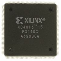
XC4013-6PQ240C
Manufacturer Part Number
XC4013-6PQ240C
Description
IC LOGIC CL ARRAY 13K GAT 240PQ
Manufacturer
Xilinx Inc
Series
XC4000r
Datasheet
1.XC4003-6PQ100C.pdf
(40 pages)
Specifications of XC4013-6PQ240C
Number Of Logic Elements/cells
1368
Number Of Labs/clbs
576
Total Ram Bits
18432
Number Of I /o
192
Number Of Gates
13000
Voltage - Supply
4.75 V ~ 5.25 V
Mounting Type
Surface Mount
Operating Temperature
0°C ~ 85°C
Package / Case
240-BFQFP
Lead Free Status / RoHS Status
Contains lead / RoHS non-compliant
Other names
122-1074
Available stocks
Company
Part Number
Manufacturer
Quantity
Price


Note:
The XC4000 families have no Powerdown control input; use the global 3-state net instead.
The XC4000 families have no dedicated Reset input. Any user I/O can be configured to drive the global Set/Reset net.
XC4000, XC4000A, XC4000H Logic Cell Array Families
Pin Descriptions
Permanently Dedicated Pins
V
Eight or more (depending on package type) connections to
the nominal +5 V supply voltage. All must be connected.
GND
Eight or more (depending on package type) connections to
ground. All must be connected.
CCLK
During configuration, Configuration Clock is an output of
the LCA in Master modes or asynchronous Peripheral
mode, but is an input to the LCA in Slave mode and
Synchronous Peripheral mode.
After configuration, CCLK has a weak pull-up resistor and
can be selected as Readback Clock.
DONE
This is a bidirectional signal, configurable with or without a
pull-up resistor of 2 to 8 k .
As an output, it indicates the completion of the configura-
tion process. The configuration program determines the
exact timing, the clock source for the Low-to-High transi-
tion, and enable of the pull-up resistor.
As an input, a Low level on DONE can be configured to
delay the global logic initialization or the enabling of
outputs
PROGRAM
This is an active Low input that forces the LCA to clear its
configuration memory.
When PROGRAM goes High, the LCA finishes the current
clear cycle and executes another complete clear cycle,
before it goes into a WAIT state and releases INIT.
CC
2-44
User I/O Pins that can have Special Functions
RDY/BUSY
During
appropriate to write another byte of data into the LCA
device. The same status is also available on D7 in asyn-
chronous peripheral mode, if a read operation is per-
formed when the device is selected. After configuration,
this is a user-programmable I/O pin.
RCLK
During Master Parallel configuration, each change on the
A0-15 outputs is preceded by a rising edge on RCLK, a
redundant output signal. After configuration, this is a user-
programmable I/O pin.
M0, M1, M2
As Mode inputs, these pins are sampled before the start of
configuration to determine the configuration mode to be
used.
After configuration, M0 and M2 can be used as inputs, and
M1 can be used as a 3-state output. These three pins have
no associated input or output registers.
These pins can be user inputs or outputs only when called
out by special schematic definitions.
TDO
If boundary scan is used, this is the Test Data Output.
If boundary scan is not used, this pin is a 3-state output
without a register, after configuration is completed.
This pin can be user output only when called out by special
schematic definitions.
TDI,TCK, TMS
If boundary scan is used, these pins are Test Data In, Test
Clock, and Test Mode Select inputs respectively coming
directly from the pads, bypassing theIOBs. These pins can
also be used as inputs to the CLB logic after configuration
is completed.
If the boundary scan option is not selected, all boundary
scan functions are inhibited once configuration is com-
pleted, and these pins become user-programmable I/O.
peripheral modes, this pin indicates when it is
Related parts for XC4013-6PQ240C
Image
Part Number
Description
Manufacturer
Datasheet
Request
R

Part Number:
Description:
IC LOGIC CL ARRAY 13K GAT 208PQ
Manufacturer:
Xilinx Inc
Datasheet:

Part Number:
Description:
IC CPLD .8K 36MCELL 44-VQFP
Manufacturer:
Xilinx Inc
Datasheet:

Part Number:
Description:
IC CPLD 72MCRCELL 10NS 44VQFP
Manufacturer:
Xilinx Inc
Datasheet:

Part Number:
Description:
IC CPLD 1.6K 72MCELL 64-VQFP
Manufacturer:
Xilinx Inc
Datasheet:

Part Number:
Description:
IC CR-II CPLD 64MCELL 44-VQFP
Manufacturer:
Xilinx Inc
Datasheet:

Part Number:
Description:
IC CPLD 1.6K 72MCELL 100-TQFP
Manufacturer:
Xilinx Inc
Datasheet:

Part Number:
Description:
IC CR-II CPLD 64MCELL 56-BGA
Manufacturer:
Xilinx Inc
Datasheet:

Part Number:
Description:
IC CPLD 72MCRCELL 7.5NS 44VQFP
Manufacturer:
Xilinx Inc
Datasheet:
Part Number:
Description:
IC CR-II CPLD 64MCELL 100-VQFP
Manufacturer:
Xilinx Inc
Datasheet:
Part Number:
Description:
IC CPLD 1.6K 72MCELL 100-TQFP
Manufacturer:
Xilinx Inc
Datasheet:

Part Number:
Description:
IC CPLD 72MCRCELL 7.5NS 64VQFP
Manufacturer:
Xilinx Inc
Datasheet:
Part Number:
Description:
IC CPLD 1.6K 72MCELL 100-TQFP
Manufacturer:
Xilinx Inc
Datasheet:

Part Number:
Description:
IC CPLD 1.5K 64MCELL HP 44-VQFP
Manufacturer:
Xilinx Inc

Part Number:
Description:
IC CPLD 36MCRCELL 15NS 44PLCC
Manufacturer:
Xilinx Inc
Datasheet:

Part Number:
Description:
IC CPLD 36MCRCELL 10NS 44PLCC
Manufacturer:
Xilinx Inc
Datasheet: