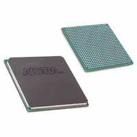
EP2S60F672C4N Altera, EP2S60F672C4N Datasheet - Page 135

EP2S60F672C4N
Manufacturer Part Number
EP2S60F672C4N
Description
IC STRATIX II FPGA 60K 672-FBGA
Manufacturer
Altera
Series
Stratix® IIr
Datasheet
1.EP2S15F484I4N.pdf
(238 pages)
Specifications of EP2S60F672C4N
Number Of Logic Elements/cells
60440
Number Of Labs/clbs
3022
Total Ram Bits
2544192
Number Of I /o
492
Voltage - Supply
1.15 V ~ 1.25 V
Mounting Type
Surface Mount
Operating Temperature
0°C ~ 85°C
Package / Case
672-FBGA
Family Name
Stratix II
Number Of Logic Blocks/elements
60440
# I/os (max)
492
Frequency (max)
711.24MHz
Process Technology
90nm (CMOS)
Operating Supply Voltage (typ)
1.2V
Logic Cells
60440
Ram Bits
2544192
Operating Supply Voltage (min)
1.15V
Operating Supply Voltage (max)
1.25V
Operating Temp Range
0C to 85C
Operating Temperature Classification
Commercial
Mounting
Surface Mount
Pin Count
672
Package Type
FC-FBGA
For Use With
544-1700 - DSP KIT W/STRATIX II EP2S60N544-1697 - NIOS II KIT W/STRATIX II EP2S60N
Lead Free Status / RoHS Status
Lead free / RoHS Compliant
Number Of Gates
-
Lead Free Status / Rohs Status
Compliant
Other names
544-1913
EP2S60F672C4N
EP2S60F672C4N
Available stocks
Company
Part Number
Manufacturer
Quantity
Price
Company:
Part Number:
EP2S60F672C4N
Manufacturer:
ALTERA
Quantity:
3 000
- Current page: 135 of 238
- Download datasheet (3Mb)
Figure 4–2. Transistor Level Diagram of FPGA Device I/O Buffers
Notes to
(1)
(2)
Power-On Reset
Circuitry
Altera Corporation
May 2007
This is the logic array signal or the larger of either the V
This is the larger of either the V
Figure
4–2:
n+
Logic Array
Stratix II devices have a POR circuit to keep the whole device system in
reset state until the power supply voltage levels have stabilized during
power-up. The POR circuit monitors the V
levels and tri-states all the user I/O pins while V
normal user levels are reached. The POR circuitry also ensures that all
eight I/O bank V
V
triggered. After the Stratix II device enters user mode, the POR circuit
continues to monitor the V
condition during user mode can be detected. If there is a V
sag below the Stratix II operational level during user mode, the POR
circuit resets the device.
When power is applied to a Stratix II device, a power-on-reset event
occurs if V
period of time (specified as a maximum V
V
dedicated input pin (PORSEL) to select POR delay times of 12 or 100 ms
during power-up. When the PORSEL pin is connected to ground, the POR
time is 100 ms. When the PORSEL pin is connected to V
is 12 ms.
p-well
Signal
CCINT
CC
CCIO
rise time for Stratix II device is 100 ms. Stratix II devices provide a
voltage, reach an acceptable level before configuration is
or V
n+
CC
PAD
reaches the recommended operating range within a certain
signal.
V
CCIO
PAD
voltages, V
CCIO
p+
CCINT
or V
PAD
(1)
voltage level so that a brown-out
CCPD
signal.
Stratix II Device Handbook, Volume 1
n-well
voltage, as well as the logic array
V
CCIO
p+
Hot Socketing & Power-On Reset
CCINT
CC
rise time). The maximum
, V
(2)
n+
CC
CCIO
p-substrate
is ramping up until
, and V
CC
, the POR time
CCINT
CCPD
voltage
voltage
4–5
Related parts for EP2S60F672C4N
Image
Part Number
Description
Manufacturer
Datasheet
Request
R

Part Number:
Description:
CYCLONE II STARTER KIT EP2C20N
Manufacturer:
Altera
Datasheet:

Part Number:
Description:
CPLD, EP610 Family, ECMOS Process, 300 Gates, 16 Macro Cells, 16 Reg., 16 User I/Os, 5V Supply, 35 Speed Grade, 24DIP
Manufacturer:
Altera Corporation
Datasheet:

Part Number:
Description:
CPLD, EP610 Family, ECMOS Process, 300 Gates, 16 Macro Cells, 16 Reg., 16 User I/Os, 5V Supply, 15 Speed Grade, 24DIP
Manufacturer:
Altera Corporation
Datasheet:

Part Number:
Description:
Manufacturer:
Altera Corporation
Datasheet:

Part Number:
Description:
CPLD, EP610 Family, ECMOS Process, 300 Gates, 16 Macro Cells, 16 Reg., 16 User I/Os, 5V Supply, 30 Speed Grade, 24DIP
Manufacturer:
Altera Corporation
Datasheet:

Part Number:
Description:
High-performance, low-power erasable programmable logic devices with 8 macrocells, 10ns
Manufacturer:
Altera Corporation
Datasheet:

Part Number:
Description:
High-performance, low-power erasable programmable logic devices with 8 macrocells, 7ns
Manufacturer:
Altera Corporation
Datasheet:

Part Number:
Description:
Classic EPLD
Manufacturer:
Altera Corporation
Datasheet:

Part Number:
Description:
High-performance, low-power erasable programmable logic devices with 8 macrocells, 10ns
Manufacturer:
Altera Corporation
Datasheet:

Part Number:
Description:
Manufacturer:
Altera Corporation
Datasheet:

Part Number:
Description:
Manufacturer:
Altera Corporation
Datasheet:

Part Number:
Description:
Manufacturer:
Altera Corporation
Datasheet:

Part Number:
Description:
CPLD, EP610 Family, ECMOS Process, 300 Gates, 16 Macro Cells, 16 Reg., 16 User I/Os, 5V Supply, 25 Speed Grade, 24DIP
Manufacturer:
Altera Corporation
Datasheet:


