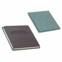
EP2S15F672C3N Altera, EP2S15F672C3N Datasheet - Page 147

EP2S15F672C3N
Manufacturer Part Number
EP2S15F672C3N
Description
IC STRATIX II FPGA 15K 672-FBGA
Manufacturer
Altera
Series
Stratix® IIr
Datasheet
1.EP2S15F484I4N.pdf
(238 pages)
Specifications of EP2S15F672C3N
Number Of Logic Elements/cells
15600
Number Of Labs/clbs
780
Total Ram Bits
419328
Number Of I /o
366
Voltage - Supply
1.15 V ~ 1.25 V
Mounting Type
Surface Mount
Operating Temperature
0°C ~ 85°C
Package / Case
672-FBGA
No. Of Macrocells
15600
Family Type
Stratix II
No. Of I/o's
366
Clock Management
DLL, PLL
I/o Supply Voltage
3.6V
Operating Frequency Max
550MHz
Rohs Compliant
Yes
Lead Free Status / RoHS Status
Lead free / RoHS Compliant
Number Of Gates
-
Other names
544-1880
EP2S15F672C3N
EP2S15F672C3N
Available stocks
Company
Part Number
Manufacturer
Quantity
Price
Company:
Part Number:
EP2S15F672C3N
Manufacturer:
ALTERA
Quantity:
500
- Current page: 147 of 238
- Download datasheet (3Mb)
Altera Corporation
April 2011
Note to
(1)
V
V
V
V
V
V
V
V
V
V
V
(DC)
V
V
(AC)
V
ΔV
V
(AC)
Symbol
Symbol
Table 5–17. SSTL-18 Class II Specifications
Table 5–18. SSTL-18 Class I & II Differential Specifications
CCIO
REF
TT
IH
IL
IH
IL
OH
OL
CCIO
SWING
X
SWING
ISO
OX
ISO
(AC) AC differential input cross
(DC) Low-level DC input voltage
(AC) Low-level AC input voltage
(DC) High-level DC input voltage
(AC) High-level AC input voltage
This specification is supported across all the programmable drive settings available for this I/O standard as shown
in the Stratix II Architecture chapter in volume 1 of the Stratix II Device Handbook.
Table
Output supply voltage
DC differential input voltage
point voltage
AC differential input voltage
Input clock signal offset
voltage
Input clock signal offset
voltage variation
AC differential cross point
voltage
Output supply voltage
Reference voltage
Termination voltage
High-level output voltage
Low-level output voltage
5–17:
Parameter
Parameter
Conditions
I
I
OH
OL
= 13.4 mA
= –13.4 mA
Conditions
(V
(V
(1)
CCIO
CCIO
(1)
Minimum
/2) – 0.175
/2) – 0.125
1.71
0.25
0.5
V
V
V
V
Minimum
REF
CCIO
REF
REF
0.855
1.71
+ 0.125
– 0.04
+ 0.25
– 0.28
Stratix II Device Handbook, Volume 1
0.5 × V
Typical
±200
1.80
DC & Switching Characteristics
CCIO
Typical
0.900
V
1.80
REF
(V
(V
CCIO
CCIO
Maximum
V
V
V
Maximum
/2) + 0.175
/2) + 0.125
REF
1.89
REF
REF
0.945
1.89
0.28
– 0.125
+ 0.04
– 0.25
5–11
Unit
Unit
mV
V
V
V
V
V
V
V
V
V
V
V
V
V
V
V
Related parts for EP2S15F672C3N
Image
Part Number
Description
Manufacturer
Datasheet
Request
R

Part Number:
Description:
CYCLONE II STARTER KIT EP2C20N
Manufacturer:
Altera
Datasheet:

Part Number:
Description:
CPLD, EP610 Family, ECMOS Process, 300 Gates, 16 Macro Cells, 16 Reg., 16 User I/Os, 5V Supply, 35 Speed Grade, 24DIP
Manufacturer:
Altera Corporation
Datasheet:

Part Number:
Description:
CPLD, EP610 Family, ECMOS Process, 300 Gates, 16 Macro Cells, 16 Reg., 16 User I/Os, 5V Supply, 15 Speed Grade, 24DIP
Manufacturer:
Altera Corporation
Datasheet:

Part Number:
Description:
Manufacturer:
Altera Corporation
Datasheet:

Part Number:
Description:
CPLD, EP610 Family, ECMOS Process, 300 Gates, 16 Macro Cells, 16 Reg., 16 User I/Os, 5V Supply, 30 Speed Grade, 24DIP
Manufacturer:
Altera Corporation
Datasheet:

Part Number:
Description:
High-performance, low-power erasable programmable logic devices with 8 macrocells, 10ns
Manufacturer:
Altera Corporation
Datasheet:

Part Number:
Description:
High-performance, low-power erasable programmable logic devices with 8 macrocells, 7ns
Manufacturer:
Altera Corporation
Datasheet:

Part Number:
Description:
Classic EPLD
Manufacturer:
Altera Corporation
Datasheet:

Part Number:
Description:
High-performance, low-power erasable programmable logic devices with 8 macrocells, 10ns
Manufacturer:
Altera Corporation
Datasheet:

Part Number:
Description:
Manufacturer:
Altera Corporation
Datasheet:

Part Number:
Description:
Manufacturer:
Altera Corporation
Datasheet:

Part Number:
Description:
Manufacturer:
Altera Corporation
Datasheet:

Part Number:
Description:
CPLD, EP610 Family, ECMOS Process, 300 Gates, 16 Macro Cells, 16 Reg., 16 User I/Os, 5V Supply, 25 Speed Grade, 24DIP
Manufacturer:
Altera Corporation
Datasheet:


