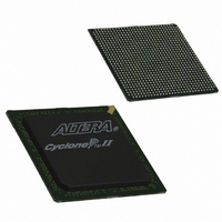
EP2C70F896I8N Altera, EP2C70F896I8N Datasheet - Page 149

EP2C70F896I8N
Manufacturer Part Number
EP2C70F896I8N
Description
IC CYCLONE II FPGA 70K 896-FBGA
Manufacturer
Altera
Series
Cyclone® IIr
Datasheet
1.EP2C5T144C8N.pdf
(168 pages)
Specifications of EP2C70F896I8N
Number Of Logic Elements/cells
68416
Number Of Labs/clbs
4276
Total Ram Bits
1152000
Number Of I /o
622
Voltage - Supply
1.15 V ~ 1.25 V
Mounting Type
Surface Mount
Operating Temperature
-40°C ~ 100°C
Package / Case
896-FBGA
Family Name
Cyclone® II
Number Of Logic Blocks/elements
68416
# I/os (max)
622
Frequency (max)
402.58MHz
Process Technology
90nm
Operating Supply Voltage (typ)
1.2V
Logic Cells
68416
Ram Bits
1152000
Operating Supply Voltage (min)
1.15V
Operating Supply Voltage (max)
1.25V
Operating Temp Range
-40C to 100C
Operating Temperature Classification
Industrial
Mounting
Surface Mount
Pin Count
896
Package Type
FBGA
For Use With
P0304 - DE2-70 CALL FOR ACADEMIC PRICING544-1703 - VIDEO KIT W/CYCLONE II EP2C70N544-1699 - DSP KIT W/CYCLONE II EPS2C70N
Lead Free Status / RoHS Status
Lead free / RoHS Compliant
Number Of Gates
-
Lead Free Status / Rohs Status
Compliant
Other names
544-2147
Available stocks
Company
Part Number
Manufacturer
Quantity
Price
Company:
Part Number:
EP2C70F896I8N
Manufacturer:
ALTERA21
Quantity:
196
Part Number:
EP2C70F896I8N
Manufacturer:
ALTERA/阿尔特拉
Quantity:
20 000
Figure 5–5. RSDS Transmitter Clock to Data Relationship
Altera Corporation
February 2008
f
(input
clock
frequency)
H S C L K
Table 5–49. Mini-LVDS Transmitter Timing Specification (Part 1 of 2)
Symbol
Conditions
rx_data[11..0]
tx_data[11..0]
At transmitter
×10
Channel-to-Channel
At receiver
×8
×7
×4
×2
×1
Skew (1.68 ns)
Table 5–49
devices at 311 Mbps. Cyclone II devices cannot receive mini-LVDS data
because the devices are intended for applications where they will be
driving display drivers. A maximum mini-LVDS data rate of 311 Mbps is
supported for Cyclone II devices using DDIO registers. Cyclone II
devices support mini-LVDS only in the commercial temperature range.
Min
10
10
10
10
10
10
–6 Speed Grade
Clock (5.88 ns)
Transmitter
Typ
—
—
—
—
—
—
t
SU
Skew
Total
(2 ns)
shows the mini-LVDS transmitter timing budget for Cyclone II
155.5
155.5
155.5
155.5
155.5
Max
311
Transmitter
Valid
Valid
Data
Data
Min
10
10
10
10
10
10
t
–7 Speed Grade
H
(2 ns)
DC Characteristics and Timing Specifications
Typ
—
—
—
—
—
—
Transmitter
Cyclone II Device Handbook, Volume 1
Valid
Valid
Data
Data
155.5
155.5
155.5
155.5
155.5
Max
311
Min
10
10
10
10
10
10
–8 Speed Grade
Typ
—
—
—
—
—
—
155.5
155.5
155.5
155.5
155.5
Max
311
MHz
MHz
MHz
MHz
MHz
MHz
Unit
5–59


