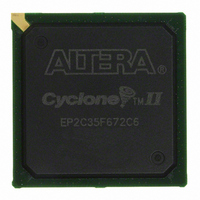
EP2C35F672C6 Altera, EP2C35F672C6 Datasheet - Page 41

EP2C35F672C6
Manufacturer Part Number
EP2C35F672C6
Description
IC CYCLONE II FPGA 33K 672-FBGA
Manufacturer
Altera
Series
Cyclone® IIr
Datasheet
1.EP2C5T144C8N.pdf
(168 pages)
Specifications of EP2C35F672C6
Number Of Logic Elements/cells
33216
Number Of Labs/clbs
2076
Total Ram Bits
483840
Number Of I /o
475
Voltage - Supply
1.15 V ~ 1.25 V
Mounting Type
Surface Mount
Operating Temperature
0°C ~ 85°C
Package / Case
672-FBGA
Family Name
Cyclone® II
Number Of Logic Blocks/elements
33216
# I/os (max)
475
Frequency (max)
500MHz
Process Technology
90nm
Operating Supply Voltage (typ)
1.2V
Logic Cells
33216
Ram Bits
483840
Operating Supply Voltage (min)
1.15V
Operating Supply Voltage (max)
1.25V
Operating Temp Range
0C to 85C
Operating Temperature Classification
Commercial
Mounting
Surface Mount
Pin Count
672
Package Type
FBGA
For Use With
P0301 - DE2 CALL FOR ACADEMIC PRICING544-1733 - PCI KIT W/CYCLONE II EP2C35N649-1001 - KIT DEV CYCLONE II PCI EXPRESS
Lead Free Status / RoHS Status
Contains lead / RoHS non-compliant
Number Of Gates
-
Lead Free Status / Rohs Status
Not Compliant
Other names
544-1087
EP2C35F672C6ES
EP2C35F672C6ES
Available stocks
Company
Part Number
Manufacturer
Quantity
Price
Company:
Part Number:
EP2C35F672C6N
Manufacturer:
ALTERA
Quantity:
170
Altera Corporation
February 2007
Note to
(1)
Maximum performance
Total RAM bits per M4K block (including parity bits)
Configurations supported
Parity bits
Byte enable
Packed mode
Address clock enable
Memory initialization file (.mif)
Power-up condition
Register clears
Same-port read-during-write
Mixed-port read-during-write
Table 2–6. M4K Memory Features
Maximum performance information is preliminary until device characterization.
Table
2–6:
Feature
(1)
Table 2–6
summarizes the features supported by the M4K memory.
250 MHz
4,608
2K × 2
1K × 4
512 × 8
512 × 9
256 × 16
256 × 18
128 × 32 (not available in true dual-port mode)
128 × 36 (not available in true dual-port mode)
One parity bit for each byte. The parity bit, along with
internal user logic, can implement parity checking for
error detection to ensure data integrity.
a data width of 1, 2, 4, 8, 9, 16, 18, 32, or 36 bits. The
byte enables allow the input data to be masked so the
device can write to specific bytes. The unwritten bytes
retain the previous written value.
Two single-port memory blocks can be packed into a
single M4K block if each of the two independent block
sizes are equal to or less than half of the M4K block
size, and each of the single-port memory blocks is
configured in single-clock mode.
used to hold the previous address value for as long as
the signal is enabled. This feature is useful in handling
misses in cache applications.
When configured as RAM or ROM, you can use an
initialization file to pre-load the memory contents.
Output registers only
New data available at positive clock edge
4K × 1
M4K blocks support byte writes when the write port has
M4K blocks support address clock enable, which is
Outputs cleared
Old data available at positive clock edge
Cyclone II Device Handbook, Volume 1
Description
Cyclone II Architecture
2–29


