EP2C35F672C6 Altera, EP2C35F672C6 Datasheet - Page 155
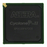
EP2C35F672C6
Manufacturer Part Number
EP2C35F672C6
Description
IC CYCLONE II FPGA 33K 672-FBGA
Manufacturer
Altera
Series
Cyclone® IIr
Datasheet
1.EP2C5T144C8N.pdf
(168 pages)
Specifications of EP2C35F672C6
Number Of Logic Elements/cells
33216
Number Of Labs/clbs
2076
Total Ram Bits
483840
Number Of I /o
475
Voltage - Supply
1.15 V ~ 1.25 V
Mounting Type
Surface Mount
Operating Temperature
0°C ~ 85°C
Package / Case
672-FBGA
Family Name
Cyclone® II
Number Of Logic Blocks/elements
33216
# I/os (max)
475
Frequency (max)
500MHz
Process Technology
90nm
Operating Supply Voltage (typ)
1.2V
Logic Cells
33216
Ram Bits
483840
Operating Supply Voltage (min)
1.15V
Operating Supply Voltage (max)
1.25V
Operating Temp Range
0C to 85C
Operating Temperature Classification
Commercial
Mounting
Surface Mount
Pin Count
672
Package Type
FBGA
For Use With
P0301 - DE2 CALL FOR ACADEMIC PRICING544-1733 - PCI KIT W/CYCLONE II EP2C35N649-1001 - KIT DEV CYCLONE II PCI EXPRESS
Lead Free Status / RoHS Status
Contains lead / RoHS non-compliant
Number Of Gates
-
Lead Free Status / Rohs Status
Not Compliant
Other names
544-1087
EP2C35F672C6ES
EP2C35F672C6ES
Available stocks
Company
Part Number
Manufacturer
Quantity
Price

Company:
Part Number:
EP2C35F672C6N
Manufacturer:
ALTERA
Quantity:
170


Altera Corporation
February 2008
Notes to
(1)
(2)
t
t
t
t
t
t
t
t
t
t
t
t
t
J C P
J C H
J C L
J P S U
J P H
J P C O
J P Z X
J P X Z
J S S U
J S H
J S C O
J S Z X
J S X Z
Table 5–53. Cyclone II JTAG Timing Parameters and Values
Symbol
This information is preliminary.
This specification is shown for 3.3-V LVTTL/LVCMOS and 2.5-V LVTTL/LVCMOS operation of the JTAG pins. For
1.8-V LVTTL/LVCMOS and 1.5-V LVCMOS, the JTAG port and capture register clock setup time is 3 ns and port
clock to output time is 15 ns.
Table
TCK
TCK
TCK
JTAG port setup time
JTAG port hold time
JTAG port clock to output
JTAG port high impedance to valid output
JTAG port valid output to high impedance
Capture register setup time
Capture register hold time
Update register clock to output
Update register high impedance to valid output
Update register valid output to high impedance
5–53:
f
clock period
clock high time
clock low time
Table 5–53
devices.
1
For more information on JTAG, refer to the
Boundary-Scan Testing for Cyclone II Devices
Handbook.
Parameter
(2)
(2)
Cyclone II devices must be within the first 17 devices in a JTAG
chain. All of these devices have the same JTAG controller. If any
of the Cyclone II devices are in the 18th position or after they will
fail configuration. This does not affect the SignalTap
analyzer.
(2)
shows the JTAG timing parameters and values for Cyclone II
(2)
(2)
DC Characteristics and Timing Specifications
Min
Cyclone II Device Handbook, Volume 1
20
20
10
10
—
—
—
—
—
—
40
5
5
chapter in the Cyclone II
IEEE 1149.1 (JTAG)
Max
13
13
13
25
25
25
—
—
—
—
—
—
—
®
II logic
Unit
ns
ns
ns
ns
ns
ns
ns
ns
ns
ns
ns
ns
ns
5–65
Related parts for EP2C35F672C6
Image
Part Number
Description
Manufacturer
Datasheet
Request
R

Part Number:
Description:
CYCLONE II STARTER KIT EP2C20N
Manufacturer:
Altera
Datasheet:


Part Number:
Description:
CPLD, EP610 Family, ECMOS Process, 300 Gates, 16 Macro Cells, 16 Reg., 16 User I/Os, 5V Supply, 35 Speed Grade, 24DIP
Manufacturer:
Altera Corporation
Datasheet:
Part Number:
Description:
CPLD, EP610 Family, ECMOS Process, 300 Gates, 16 Macro Cells, 16 Reg., 16 User I/Os, 5V Supply, 15 Speed Grade, 24DIP
Manufacturer:
Altera Corporation
Datasheet:
Part Number:
Description:
Manufacturer:
Altera Corporation
Datasheet:
Part Number:
Description:
CPLD, EP610 Family, ECMOS Process, 300 Gates, 16 Macro Cells, 16 Reg., 16 User I/Os, 5V Supply, 30 Speed Grade, 24DIP
Manufacturer:
Altera Corporation
Datasheet:
Part Number:
Description:
High-performance, low-power erasable programmable logic devices with 8 macrocells, 10ns
Manufacturer:
Altera Corporation
Datasheet:
Part Number:
Description:
High-performance, low-power erasable programmable logic devices with 8 macrocells, 7ns
Manufacturer:
Altera Corporation
Datasheet:
Part Number:
Description:
Classic EPLD
Manufacturer:
Altera Corporation
Datasheet:
Part Number:
Description:
High-performance, low-power erasable programmable logic devices with 8 macrocells, 10ns
Manufacturer:
Altera Corporation
Datasheet:
Part Number:
Description:
Manufacturer:
Altera Corporation
Datasheet:
Part Number:
Description:
Manufacturer:
Altera Corporation
Datasheet:
Part Number:
Description:
Manufacturer:
Altera Corporation
Datasheet:
Part Number:
Description:
CPLD, EP610 Family, ECMOS Process, 300 Gates, 16 Macro Cells, 16 Reg., 16 User I/Os, 5V Supply, 25 Speed Grade, 24DIP
Manufacturer:
Altera Corporation
Datasheet: