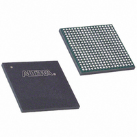
EP1C12F324C6 Altera, EP1C12F324C6 Datasheet - Page 53

EP1C12F324C6
Manufacturer Part Number
EP1C12F324C6
Description
IC CYCLONE FPGA 12K LE 324-FBGA
Manufacturer
Altera
Series
Cyclone®r
Datasheet
1.EP1C3T144C8.pdf
(106 pages)
Specifications of EP1C12F324C6
Number Of Logic Elements/cells
12060
Number Of Labs/clbs
1206
Total Ram Bits
239616
Number Of I /o
249
Voltage - Supply
1.425 V ~ 1.575 V
Mounting Type
Surface Mount
Operating Temperature
0°C ~ 85°C
Package / Case
324-FBGA
Family Name
Cyclone®
Number Of Logic Blocks/elements
12060
# I/os (max)
249
Frequency (max)
405.2MHz
Process Technology
0.13um (CMOS)
Operating Supply Voltage (typ)
1.5V
Logic Cells
12060
Ram Bits
239616
Operating Supply Voltage (min)
1.425V
Operating Supply Voltage (max)
1.575V
Operating Temp Range
0C to 85C
Operating Temperature Classification
Commercial
Mounting
Surface Mount
Pin Count
324
Package Type
FBGA
Lead Free Status / RoHS Status
Contains lead / RoHS non-compliant
Number Of Gates
-
Lead Free Status / Rohs Status
Not Compliant
Other names
544-1034
Available stocks
Company
Part Number
Manufacturer
Quantity
Price
Company:
Part Number:
EP1C12F324C6
Manufacturer:
ALTERA
Quantity:
7
Company:
Part Number:
EP1C12F324C6
Manufacturer:
ALTERA
Quantity:
1 831
Company:
Part Number:
EP1C12F324C6
Manufacturer:
ALTERA
Quantity:
210
Company:
Part Number:
EP1C12F324C6AA
Manufacturer:
ALTERA
Quantity:
3 000
Company:
Part Number:
EP1C12F324C6N
Manufacturer:
ALTERA
Quantity:
5
Figure 2–33. Cyclone Device DQ and DQS Groups in ×8 Mode
Note to
(1)
Altera Corporation
May 2008
Each DQ group consists of one DQS pin, eight DQ pins, and one DM pin.
Figure
Top, Bottom, Left, or Right I/O Bank
2–33:
output pins (nSTATUS and CONF_DONE) and all the JTAG pins in I/O
bank 3 must operate at 2.5 V because the V
I/O banks 1, 2, 3, and 4 support DQS signals with DQ bus modes of × 8.
For × 8 mode, there are up to eight groups of programmable DQS and DQ
pins, I/O banks 1, 2, 3, and 4 each have two groups in the 324-pin and
400-pin FineLine BGA packages. Each group consists of one DQS pin, a
set of eight DQ pins, and one DM pin (see
drives the set of eight DQ pins within that group.
Table 2–10
EP1C3
EP1C4
Table 2–10. DQ Pin Groups (Part 1 of 2)
Device
DQ Pins
shows the number of DQ pin groups per device.
100-pin TQFP
144-pin TQFP
324-pin FineLine BGA
400-pin FineLine BGA
DQS Pin
Package
(1)
Note (1)
Number of × 8 DQ
Pin Groups
Figure
CCIO
3
4
8
8
level of SSTL-2 is 2.5 V.
2–33). Each DQS pin
DM Pin
Total DQ Pin
I/O Structure
Count
Preliminary
24
32
64
64
2–47


