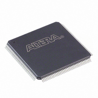
EP1C6T144C7N Altera, EP1C6T144C7N Datasheet - Page 46

EP1C6T144C7N
Manufacturer Part Number
EP1C6T144C7N
Description
IC CYCLONE FPGA 5980 LE 144-TQFP
Manufacturer
Altera
Series
Cyclone®r
Datasheet
1.EP1C3T144C8.pdf
(106 pages)
Specifications of EP1C6T144C7N
Number Of Logic Elements/cells
5980
Number Of Labs/clbs
598
Total Ram Bits
92160
Number Of I /o
98
Voltage - Supply
1.425 V ~ 1.575 V
Mounting Type
Surface Mount
Operating Temperature
0°C ~ 85°C
Package / Case
144-TQFP, 144-VQFP
Family Name
Cyclone®
Number Of Logic Blocks/elements
5980
# I/os (max)
98
Frequency (max)
320.1MHz
Process Technology
0.13um (CMOS)
Operating Supply Voltage (typ)
1.5V
Logic Cells
5980
Ram Bits
92160
Operating Supply Voltage (min)
1.425V
Operating Supply Voltage (max)
1.575V
Operating Temp Range
0C to 85C
Operating Temperature Classification
Commercial
Mounting
Surface Mount
Pin Count
144
Package Type
TQFP
Lead Free Status / RoHS Status
Lead free / RoHS Compliant
Number Of Gates
-
Lead Free Status / Rohs Status
Compliant
Other names
544-1816
EP1C6T144C7N
EP1C6T144C7N
Available stocks
Company
Part Number
Manufacturer
Quantity
Price
Company:
Part Number:
EP1C6T144C7N
Manufacturer:
ALTERA
Quantity:
23
Company:
Part Number:
EP1C6T144C7N
Manufacturer:
ALT
Quantity:
5 510
Company:
Part Number:
EP1C6T144C7N
Manufacturer:
ALTERA
Quantity:
648
Part Number:
EP1C6T144C7N
Manufacturer:
ALTERA
Quantity:
20 000
Cyclone Device Handbook, Volume 1
2–40
Preliminary
Figure 2–27. Cyclone IOE Structure
Note to
(1)
The IOEs are located in I/O blocks around the periphery of the Cyclone
device. There are up to three IOEs per row I/O block and up to three IOEs
per column I/O block (column I/O blocks span two columns). The row
I/O blocks drive row, column, or direct link interconnects. The column
I/O blocks drive column interconnects.
I/O block connects to the logic array.
I/O block connects to the logic array.
There are two paths available for combinatorial inputs to the logic array. Each path
contains a unique programmable delay chain.
Figure
Logic Array
Combinatorial
2–27:
input (1)
Output
Input
OE
Output Register
Input Register
OE Register
D
D
D
Figure 2–29
Q
Q
Q
Figure 2–28
shows how a column
shows how a row
Altera Corporation
May 2008


