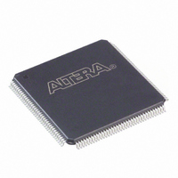
EP1C3T144C8 Altera, EP1C3T144C8 Datasheet - Page 55

EP1C3T144C8
Manufacturer Part Number
EP1C3T144C8
Description
IC CYCLONE FPGA 2910 LE 144-TQFP
Manufacturer
Altera
Series
Cyclone®r
Datasheet
1.EP1C3T144C8.pdf
(106 pages)
Specifications of EP1C3T144C8
Number Of Logic Elements/cells
2910
Number Of Labs/clbs
291
Total Ram Bits
59904
Number Of I /o
104
Voltage - Supply
1.425 V ~ 1.575 V
Mounting Type
Surface Mount
Operating Temperature
0°C ~ 85°C
Package / Case
144-TQFP, 144-VQFP
Family Name
Cyclone®
Number Of Logic Blocks/elements
2910
# I/os (max)
104
Frequency (max)
275.03MHz
Process Technology
0.13um (CMOS)
Operating Supply Voltage (typ)
1.5V
Logic Cells
2910
Ram Bits
59904
Operating Supply Voltage (min)
1.425V
Operating Supply Voltage (max)
1.575V
Operating Temp Range
0C to 85C
Operating Temperature Classification
Commercial
Mounting
Surface Mount
Pin Count
144
Package Type
TQFP
Lead Free Status / RoHS Status
Contains lead / RoHS non-compliant
Number Of Gates
-
Lead Free Status / Rohs Status
Not Compliant
Other names
544-1052
Available stocks
Company
Part Number
Manufacturer
Quantity
Price
Company:
Part Number:
EP1C3T144C8
Manufacturer:
ALTERA
Quantity:
13
Company:
Part Number:
EP1C3T144C8
Manufacturer:
ALTERA
Quantity:
266
Company:
Part Number:
EP1C3T144C8
Manufacturer:
ALTERA
Quantity:
853
Part Number:
EP1C3T144C8
Manufacturer:
ALTERA/阿尔特拉
Quantity:
20 000
Company:
Part Number:
EP1C3T144C8N
Manufacturer:
Altera
Quantity:
1 994
Company:
Part Number:
EP1C3T144C8N
Manufacturer:
ALTERA
Quantity:
1 235
Part Number:
EP1C3T144C8N
Manufacturer:
ALTERA/阿尔特拉
Quantity:
20 000
Figure 2–34. DDR SDRAM and FCRAM Interfacing
Altera Corporation
May 2008
PLL
OE
Phase Shifted -90˚
Register
OE LE
Register
OE LE
GND
V
CC
Output LE
Output LE
Register
Register
Programmable Drive Strength
The output buffer for each Cyclone device I/O pin has a programmable
drive strength control for certain I/O standards. The LVTTL and
LVCMOS standards have several levels of drive strength that the designer
can control. SSTL-3 class I and II, and SSTL-2 class I and II support a
minimum setting, the lowest drive strength that guarantees the I
Programmable
Delay Chain
clk
DQS
Δ t
OE
Register
OE LE
Global Clock
Register
OE LE
DataA
DataB
Output LE
Output LE
Registers
Registers
-90˚ clk
DQ
Adjacent LAB LEs
Register
Register
LE
LE
Registers
Registers
Input LE
Input LE
I/O Structure
Preliminary
Adjacent
LAB LEs
Resynchronizing
Global Clock
OH
/I
2–49
OL


