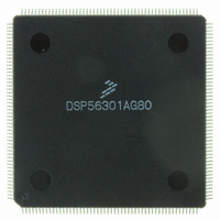
DSP56301AG80 Freescale Semiconductor, DSP56301AG80 Datasheet - Page 2

DSP56301AG80
Manufacturer Part Number
DSP56301AG80
Description
IC DSP 24BIT 80MHZ GP 208-LQFP
Manufacturer
Freescale Semiconductor
Series
DSP563xxr
Type
Fixed Pointr
Specifications of DSP56301AG80
Interface
Host Interface, SSI, SCI
Clock Rate
80MHz
Non-volatile Memory
ROM (9 kB)
On-chip Ram
24kB
Voltage - I/o
3.30V
Voltage - Core
3.30V
Operating Temperature
-40°C ~ 100°C
Mounting Type
Surface Mount
Package / Case
208-LQFP
Lead Free Status / RoHS Status
Lead free / RoHS Compliant
Available stocks
Company
Part Number
Manufacturer
Quantity
Price
Company:
Part Number:
DSP56301AG80
Manufacturer:
CONEXANT
Quantity:
4 200
Company:
Part Number:
DSP56301AG80
Manufacturer:
FREESCALE
Quantity:
7
Company:
Part Number:
DSP56301AG80
Manufacturer:
Freescale Semiconductor
Quantity:
10 000
Company:
Part Number:
DSP56301AG80B1
Manufacturer:
Freescale Semiconductor
Quantity:
10 000
DSP56301 Features
DSP56301 Features
•
•
•
•
•
2
High-performance DSP56300 core
— 66/80/100 Million Instructions Per Second (MIPS) with a 66/80/100 MHz clock at 3.3 V
— Object code compatible with the DSP56000 core
— Highly parallel instruction set
— Fully pipelined 24 x 24-bit parallel multiplier-accumulator
— 56-bit parallel barrel shifter
— 24-bit or 16-bit arithmetic support under software control
— Position independent code support
— Addressing modes optimized for DSP applications
— On-chip instruction cache controller
— On-chip memory-expandable hardware stack
— Nested hardware DO loops
— Fast auto-return interrupts
— On-chip concurrent six-channel DMA controller
— On-chip Phase Lock Loop (PLL) and clock generator
— On-Chip Emulation (OnCE™) module
— Joint Action Test Group (JTAG) Test Access Port (TAP)
— Address tracing mode that reflects internal accesses at the external port
On-chip memories
— Program RAM, Instruction Cache, X data RAM, and Y data RAM size are programmable:
— 192 × 24-bit bootstrap ROM
Off-chip memory expansion
— Data memory expansion to two 16 M x 24-bit word memory spaces
— Program memory expansion to one 16 M x 24-bit word memory space
— External memory expansion port
— Chip Select Logic requiring no additional circuitry to interface to SRAMs and SSRAMs
— On-chip DRAM controller that requires no additional circuitry to interface to DRAMs
On-chip peripherals
— 32-bit parallel PCI/Universal Host Interface (HI32), PCI Rev. 2.1 compliant with no additional interface logic
— ISA interface requires only 74LS45-style buffer
— Two Enhanced Synchronous Serial Interfaces (ESSI)
— Serial Communications Interface (SCI) with baud rate generator
— Triple timer module
— Up to 42 programmable General Purpose I/O pins (GPIO), depending on which peripherals are enabled
Reduced power dissipation
— Very low power CMOS design
— Wait and Stop low power standby modes
— Fully-static logic, operation frequency down to 0 Hz (DC)
— Optimized power management circuitry
required for other DSP563xx buses
Instruction
disabled
disabled
enabled
enabled
Cache
disabled
disabled
enabled
enabled
Switch
Mode
4096 × 24-bit
3072 × 24-bit
2048 × 24-bit
1024 × 24-bit
RAM Size
Program
DSP56301 Product Brief, Rev. 2
1024 × 24-bit
1024 × 24-bit
Instruction
Cache Size
0
0
X Data RAM
2048 × 24-bit
2048 × 24-bit
3072 × 24-bit
3072 × 24-bit
Size
2048 × 24-bit
2048 × 24-bit
3072 × 24-bit
3072 × 24-bit
Y Data Ram
Freescale Semiconductor
Size


