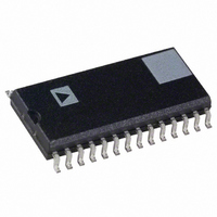
ADMCF327BR Analog Devices Inc, ADMCF327BR Datasheet - Page 18

ADMCF327BR
Manufacturer Part Number
ADMCF327BR
Description
IC DSP SW MOTOR CTRLR 28SOIC
Manufacturer
Analog Devices Inc
Series
Motor Controlr
Type
Fixed Pointr
Datasheet
1.ADMCF327BR.pdf
(36 pages)
Specifications of ADMCF327BR
Rohs Status
RoHS non-compliant
Interface
Synchronous Serial Port (SSP)
Clock Rate
20MHz
Non-volatile Memory
FLASH (12 kB), ROM (12kB)
On-chip Ram
2.5kB
Voltage - I/o
5.00V
Voltage - Core
5.00V
Operating Temperature
-40°C ~ 85°C
Mounting Type
Surface Mount
Package / Case
28-SOIC (7.5mm Width)
Lead Free Status / Rohs Status
Not Compliant
ADMCF327
The ADC system consists of four comparators and a single
timer, which may be clocked at either the DSP rate or half the
DSP rate, depending on the setting of the ADCCNT bit (Bit 7)
of the MODECTRL register. When this bit is cleared, the timers
count at a slower rate of CLKIN. When this bit is set, they count
at CLKOUT or twice the rate of CLKIN. ADC1, ADC2, ADC3,
and ADCAUX are the registers that capture the conversion
times, which are effectively the timer values, when the associated
comparator trips.
ADC Resolution
The ADC is intrinsically linked to the PWM block through the
PWMSYNC pulse controlling the ADC conversion process.
Because of this link, the effective resolution of the ADC is a
function of both the PWM switching frequency and the rate
at which the ADC counter timer is clocked. For a CLKOUT
period of t
the ADC is given by:
COMPARATOR
PWMSYNC
OUTPUT
V
VIL
200
150
100
50
Max Count = min (4095, (T
0
Max Count = min (4095, (T
CK
0
and a PWM period of T
2
t
T
VIL
for MODECTRL Bit 7 = 0
for MODECTRL Bit 7 = 1
PWM
CHARGING CAPACITOR – nF
–T
CRST
V
C
4
PWM
PWM
PWM
6
, the maximum count of
– T
– T
V
T
CMAX
CRST
CRST
CRST
8
)/2 t
)/t
CK
CK
)
)
10
t
V1
Where T
update mode, or it is equal to half that period if operating in
double update mode. For an assumed CLKOUT frequency of
20 MHz and PWMSYNC pulsewidth of 2.0 µs, the effective
resolution of the ADC block is tabulated for various PWM
switching frequencies in Table VII.
PWM
Frequency
(kHz)
2.4
4
8
18
25
Charging Capacitor Selection
The charging capacitor value is selected based on the sample
(PWM) frequency desired. A too-small capacitor value will reduce
the available resolution of the ADC by having the ramp voltage
rise rapidly and convert too quickly, not utilizing all possible
counts available in the PWM cycle. Too large a capacitor may not
convert in the available PWM cycle returning 0x000. To select a
charging capacitor, use Figure 14, select the sampling frequency
desired, determine if the current source is to be tuned to a nominal
100 µA or left in the default (0x0 code) trim state, then determine
the proper charge capacitor off the appropriate curve.
Programmable Current Source
The ADMCF327 has an internal current source that is used to
charge an external capacitor, generating the voltage ramp used
for conversion. The magnitude of the output of the current
source circuit is subject to manufacturing variations and can
vary from one device to the next. Therefore, the ADMCF327
incudes a programmable current source whose output can always
be tuned to within 5% of the target 100 µA. A 3-bit register,
ICONST_TRIM, allows the user to make this adjustment. The
output current is proportional to the value written to the regis-
ter: 0x0 produces the minimum output, and 0x7 produces the
maximum output. The default value of ICONST_TRIM after
reset is 0x0.
100
10
PWM
1
1
Table VII. ADC Resolution Examples
DEFAULT ICONST
is equal to the PWM period if operating in single
MODECTRL[7] = 0
Max
Count
4095
2480
1230
535
380
TUNED ICONST
Effective
Resolution
12
>11
>10
>9
>8
FREQUENCY – kHz
10
MODECTRL[7] = 1
Max
Count
4095
4095
2460
1070
760
Effective
Resolution
12
12
>11
>10
>9
100


