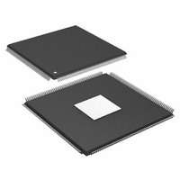
ADSP-21375KSWZ-2B Analog Devices Inc, ADSP-21375KSWZ-2B Datasheet - Page 26

ADSP-21375KSWZ-2B
Manufacturer Part Number
ADSP-21375KSWZ-2B
Description
IC DSP 32BIT 266MHZ 208-MQFP
Manufacturer
Analog Devices Inc
Series
SHARC®r
Type
Floating Pointr
Specifications of ADSP-21375KSWZ-2B
Package / Case
208-LQFP
Interface
DAI, DPI
Operating Temperature
0°C ~ 70°C
Clock Rate
266MHz
Non-volatile Memory
ROM (256 kB)
On-chip Ram
64kB
Voltage - I/o
3.30V
Voltage - Core
1.20V
Mounting Type
Surface Mount
Svhc
No SVHC (18-Jun-2010)
Base Number
21375
Core Frequency Typ
266MHz
Dsp Type
Floating Point
Mmac
532
No. Of Pins
208
Interface Type
SPI, UART
Rohs Compliant
Yes
Operating Temperature Range
0°C To +70°C
Package
208LQFP EP
Numeric And Arithmetic Format
Floating-Point
Maximum Speed
266 MHz
Ram Size
64 KB
Device Million Instructions Per Second
266 MIPS
Lead Free Status / RoHS Status
Lead free / RoHS Compliant
Available stocks
Company
Part Number
Manufacturer
Quantity
Price
Company:
Part Number:
ADSP-21375KSWZ-2B
Manufacturer:
BB
Quantity:
116
Company:
Part Number:
ADSP-21375KSWZ-2B
Manufacturer:
Analog Devices Inc
Quantity:
10 000
ADSP-21371/ADSP-21375
Precision Clock Generator (Direct Pin Routing)
This timing is only valid when the SRU is configured such that
the precision clock generator (PCG) takes its inputs directly
from the DAI pins (via pin buffers) and sends its outputs
directly to the DAI pins. For the other cases, where the PCG’s
Table 24. Precision Clock Generator (Direct Pin Routing)
1
Parameter
Timing Requirements
t
t
t
Switching Characteristics
t
t
t
t
D = FSxDIV, PH = FSxPHASE. For more information, see the ADSP-2136x SHARC Processor Hardware Reference for the ADSP-21368 Processor,
“Precision Clock Generators” chapter.
Normal mode of operation.
PCGIW
STRIG
HTRIG
DPCGIO
DTRIGCLK
DTRIGFS
PCGOW
1
Input Clock Period
PCG Trigger Setup Before Falling Edge of
PCG Input Clock
PCG Trigger Hold After Falling Edge of PCG
Input Clock
PCG Output Clock and Frame Sync Active
Edge Delay After PCG Input Clock
PCG Output Clock Delay After PCG Trigger 2.5 + ((2.5) × t
PCG Frame Sync Delay After PCG Trigger
Output Clock Period
PCG_TRIGx_I
PCG_CLKx_O
PCG_EXTx_I
PCG_FSx_O
DAI_Pn
DPI_Pn
DAI_Py
DPI_Py
DAI_Pm
DPI_Pm
(CLKIN)
DAI_Pz
DPI_Pz
t
STRIG
Figure 14. Precision Clock Generator (Direct Pin Routing)
Rev. B | Page 26 of 52 | June 2008
t
t
DTRIGCLK
DPCGIO
t
HTRIG
t
DTRIGFS
1.2 V, 266 MHz
Min
24
4.5
3
2.5
2.5 + ((2.5 + D – PH) × t
2 × t
PCGIW
– 1
t
t
inputs and outputs are not directly routed to/from DAI pins (via
pin buffers) there is no timing data available. All timing param-
eters and switching characteristics apply to external DAI pins
(DAI_P01–DAI_P20).
DPCGIO
PCGIW
PCGIW
)
PCGIW
) 10 + ((2.5 + D – PH) × t
Max
10
10 + ((2.5) × t
t
PCGOW
PCGIW
)
PCGIW
) ns
Unit
ns
ns
ns
ns
ns
ns


