CY7C372I-100JC Cypress Semiconductor Corp, CY7C372I-100JC Datasheet - Page 3
CY7C372I-100JC
Manufacturer Part Number
CY7C372I-100JC
Description
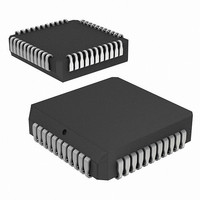
IC CPLD 64 MACROCELL 44-PLCC
Manufacturer
Cypress Semiconductor Corp
Series
Ultralogic™r
Specifications of CY7C372I-100JC
Memory Type
FLASH
Programmable Type
In-System Reprogrammable™ (ISR™) Flash
Delay Time Tpd(1) Max
12.0ns
Voltage Supply - Internal
4.75 V ~ 5.25 V
Number Of Logic Elements/blocks
4
Number Of Macrocells
64
Number Of I /o
32
Operating Temperature
0°C ~ 70°C
Mounting Type
Surface Mount
Package / Case
44-PLCC
Voltage
3.3V/5V
Family Name
FLASH370i
# Macrocells
64
Number Of Usable Gates
1600
Propagation Delay Time
12ns
Number Of Logic Blocks/elements
4
# I/os (max)
32
Operating Supply Voltage (typ)
5V
In System Programmable
Yes
Operating Supply Voltage (min)
4.75V
Operating Supply Voltage (max)
5.25V
Operating Temp Range
0C to 70C
Operating Temperature Classification
Commercial
Mounting
Surface Mount
Pin Count
44
Package Type
PLCC
Lead Free Status / RoHS Status
Contains lead / RoHS non-compliant
Features
-
Number Of Logic Elements/cells
-
Lead Free Status / RoHS Status
Not Compliant, Contains lead / RoHS non-compliant
Other names
428-1268
Available stocks
Company
Part Number
Manufacturer
Quantity
Price
Company:

Part Number:
CY7C372I-100JC
Manufacturer:
CY
Quantity:
101
Company:
Part Number:
CY7C372I-100JC
Manufacturer:
CY
Quantity:
1


PCI Compliance
The F
the PCI Local Bus Specification published by the PCI Special
Interest Group. The simple and predictable timing model of
F
independent of the design. On the other hand, in CPLD and
FPGA architectures without simple and predictable timing, PCI
compliance is dependent upon routing and product term dis-
tribution.
3.3V or 5.0V I/O operation
The F
3.3V and 5.0V systems. All devices have two sets of V
one set, V
another set, V
always be connected to a 5.0V power supply. However, the
V
supply, depending on the output requirements. When V
pins are connected to a 5.0V source, the I/O voltage levels are
compatible with 5.0V systems. When V
ed to a 3.3V source, the input voltage levels are compatible
with both 5.0V and 3.3V systems, while the output voltage lev-
els are compatible with 3.3V systems. There will be an addi-
tional timing delay on all output buffers when operating in 3.3V
I/O mode. The added flexibility of 3.3V I/O capability is avail-
able in commercial and industrial temperature ranges.
Bus Hold Capabilities on all I/Os and Dedicated Inputs
In addition to ISR capability, a new feature called bus-hold has
been added to all F
Bus-hold, which is an improved version of the popular internal
pull-up resistor, is a weak latch connected to the pin that does
not degrade the device’s performance. As a latch, bus-hold
recalls the last state of a pin when it is three-stated, thus re-
Operating Range
Note:
Document #: 38-03033 Rev. **
2.
Commercial
Industrial
Military
LASH
CCIO
T
A
Range
LASH
370i ensures compliance with the PCI AC specifications
LASH
pins may be connected to either a 3.3V or 5.0V power
is the “instant on” case temperature.
[2]
370i family of CMOS CPLDs are fully compliant with
CCINT
370i family can be configured to operate in both
CCIO
, for internal operation and input buffers, and
, for I/O output drivers. V
LASH
–55°C to +125°C
Temperature
0 C to +70 C
40 C to +85 C
370i I/Os and dedicated input pins.
Ambient
CCIO
pins are connect-
CCINT
5V
5V
5V
V
V
CCINT
pins must
CC
0.25V
0.5V
0.5V
CC
pins:
CCIO
3.3V
3.3V
5V
ducing system noise in bus-interface applications. Bus-hold
additionally allows unused device pins to remain unconnected
on the board, which is particularly useful during prototyping as
designers can route new signals to the device without cutting
trace connections to V
Design Tools
Development software for the CY7C372i is available from
Cypress’s Warp™, Warp Professional™, and Warp Enter-
prise™ software packages. Please refer to the data sheets on
these products for more details. Cypress also actively sup-
ports almost all third-party design tools. Please refer to
third-party tool support for further information.
Maximum Ratings
(Above which the useful life may be impaired. For user guide-
lines, not tested.)
Storage Temperature ................................. –65 C to +150 C
Ambient Temperature with
Power Applied ............................................ –55 C to +125 C
Supply Voltage to Ground Potential ...............–0.5V to +7.0V
DC Voltage Applied to Outputs
in High Z State................................................–0.5V to +7.0V
DC Input Voltage ............................................–0.5V to +7.0V
DC Program Voltage .................................................... 12.5V
Output Current into Outputs ........................................ 16 mA
Static Discharge Voltage ........................................... >2001V
(per MIL–STD–883, Method 3015)
Latch-Up Current..................................................... >200 mA
5V
V
OR
OR
CCIO
0.25V
0.5V
0.3V
0.3V
CC
or GND.
CY7C372i
Page 3 of 12
Related parts for CY7C372I-100JC
Image
Part Number
Description
Manufacturer
Datasheet
Request
R

Part Number:
Description:
Manufacturer:
Cypress Semiconductor Corp
Datasheet:

Part Number:
Description:
Manufacturer:
Cypress Semiconductor Corp
Datasheet:
Part Number:
Description:
Manufacturer:
Cypress Semiconductor Corp
Datasheet:
Part Number:
Description:
Manufacturer:
Cypress Semiconductor Corp
Datasheet:
Part Number:
Description:
Manufacturer:
Cypress Semiconductor Corp
Datasheet:
Part Number:
Description:
Manufacturer:
Cypress Semiconductor Corp
Datasheet:
Part Number:
Description:
Manufacturer:
Cypress Semiconductor Corp
Datasheet: