CY7C371I-110JC Cypress Semiconductor Corp, CY7C371I-110JC Datasheet
CY7C371I-110JC
Specifications of CY7C371I-110JC
Available stocks


Related parts for CY7C371I-110JC


CY7C371I-110JC Summary of contents
Page 1
... Like all members of the F in I/O resources. Each macrocell in the device features an as- sociated I/O pin, resulting in 32 I/O pins on the CY7C371i. In addition, there are three dedicated inputs and two input/clock pins. CLOCK ...
Page 2
... I/O pin is used as an input. Programmable Interconnect Matrix The Programmable Interconnect Matrix (PIM) connects the two logic blocks on the CY7C371i to the inputs and to each other. All inputs (including feedbacks) travel through the PIM. There is no speed penalty incurred by signals traversing the PIM ...
Page 3
... Document #: 38-03032 Rev. ** Design Tools pins must CCINT Development software for the CY7C371i is available from Cypress’s Warp™, Warp Professional™, and Warp Enter- prise™ software packages. Please refer to the data sheets on CCIO these products for more details. Cypress also actively sup- ports almost all third-party design tools ...
Page 4
... V = Min 2. Max Max. CC Test Conditions V = 5.0V at f=1 MHz 5. MHz IN Test Conditions MHz IN Test Conditions Normal Programming Conditions =V CC CY7C371i Min. Typ. [4] 2.4 [4,5] A (Com’l/Ind) [4,5] [4] [6] 2.0 [6] 0 [5] 0 –70 30 Com’l/Ind. 75 Com’l “L” 66 +75 75 Min. Max. ...
Page 5
... OUTPUT 5 pF INCLUDING JIG AND (b) SCOPE 3.0V GND 2.08V(COM'L) < 2.13V(MIL) Output Waveform Measurement Level V OH 0. 0.5V measured with 35-pF AC Test Load. EA CY7C371i 170 (COM'L) 236 (MIL) 7c371i–5 ALL INPUT PULSES 90% 90% 10% ( 10% < 7c371i–6 Page ...
Page 6
... All AC parameters are measured with 16 outputs switching and 35-pF AC Test Load. 13. This specification is intended to guarantee interface compatibility of the other members of the CY7C370i family with the CY7C371i. This specification is met for the devices operating at the same ambient temperature and at the same power supply voltage. ...
Page 7
... INPUT LATCH ENABLE LATCHED OUTPUT Document #: 38-03032 Rev. ** [12] (continued) 7C371i 143 Min. Max. 7 125 , 1/( ICS WL WH [8] 8 [8] 10 [1] 14 [8] 8 [8] 10 [1] 14 500 PDL CY7C371i 7C371i 83 7C371i 66 7C371i 110 7C371iL 83 7C371iL 66 Min. Max. Min. Max. Min 111 76.9 62 500 500 500 Max ...
Page 8
... OUTPUT CLOCK Clock to Clock REGISTERED INPUT INPUT REGISTER CLOCK OUTPUT REGISTER CLOCK Latched Input LATCHED INPUT LATCH ENABLE COMBINATORIAL OUTPUT LATCH ENABLE Document #: 38-03032 Rev ICS PDL t WH CY7C371i IH t ICO SCS t ICO t WL 7c371i–9 7c371i–10 7c371i–11 Page ...
Page 9
... Latched Input and Output LATCHED INPUT LATCHED OUTPUT INPUT LATCH ENABLE OUTPUT LATCH ENABLE LATCH ENABLE Asynchronous Reset INPUT REGISTERED OUTPUT CLOCK Asynchronous Preset INPUT REGISTERED OUTPUT CLOCK Document #: 38-03032 Rev ICOL t ICS CY7C371i t PDLL 7c371i– 7c371i– 7c371i–14 Page ...
Page 10
... CY7C371i 83JC CY7C371i 83AI CY7C371i 83JI CY7C371iL 83AC CY7C371iL 83JC CY7C371iL 83AI CY7C371iL 83JI 66 CY7C371i 66AC CY7C371i 66JC CY7C371i 66AI CY7C371i 66JI CY7C371iL 66AC CY7C371iL 66JC CY7C371iL 66AI CY7C371iL 66JI F 370, F 370i, ISR, UltraLogic, Warp, Warp Professional, and Warp Enterprise are trademarks of Cypress Semiconductor ...
Page 11
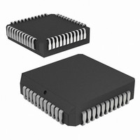
... The inclusion of Cypress Semiconductor products in life-support systems application implies that the manufacturer assumes all risk of such use and in doing so indemnifies Cypress Semiconductor against all charges. 44-Lead Thin Plastic Quad Flat Pack A44 44-Lead Plastic Leaded Chip Carrier J67 CY7C371i 51-85064-B 51-85003-A Page ...
Page 12
... Document Title: CY7C371i UltraLogic™ 32-Macrocell Flash CPLD Document Number: 38-03032 REV. ECN NO. Issue Date ** 106377 06/18/01 Document #: 38-03032 Rev. ** Orig. of Change SZV Change from Spec #: 38-00497 to 38-03032 CY7C371i Description of Change Page ...